Scanning Electron Microscope


If you want to visualize the smallest structures, scanning electron microscopy is the way to do it. As electrons have a much shorter wavelength than visible light, much smaller details can be resolved in the sample. Electron microscopes have evolved over the past decade, from complicated and large machines to easy to use technology that now even exists in desktop format. ST Instruments provides a range of scanning electron microscope equipment from Hitachi High-Tech to suit different requirements. Our instruments allow you to study a wide range of samples, from biological samples to polymers, semiconductors, or other advanced materials. We also provide equipment for sample preparation.

SEM

♦    SU8600 | High-brightness cold field emission source provides ultrahigh-resolution images even at Ultra-low voltages

♦    SU9000 | Features the world’s highest SE resolution of 0.4 nm at 30 kV

♦    SU8700 | Characterized by its Ultrahigh-Resolution and Analytical Capability

♦    SU7000 | Characterized by its versatile imaging capacity

♦    SU5000 | With revolutionary computer-assisted EM Wizard technology

♦    SU3800 | VP-SEM with thermionic electron source

♦    SU3900 | VP-SEM with thermionic electron source and large sample chamber

Desktop SEM

Table-top SEM TM4000

♦    TM4000Plus II | With a high-sensitivity low-vacuum SE detector

♦    TM4000 II | Integrates ease of use, optimized imaging, and high-image quality

♦    FlexSEM 1000 II | Compact variable-pressure SEM with unparalleled image resolution

FIB-SEM

Scanning Electron Microscope Ethos

♦    ETHOS | State-of-the-art imaging performance

♦    NX9000 | Optimal for 3D structural analysis

♦    NX2000 | For high throughput and high quality TEM sample preparation

TEM

Transmission Electron Microscope HT7800

♦    HT7800 | With multiple lens configurations and automated image stitching

♦    HF5000 | unique 200 kV aberration-corrected TEM/STEM

Sample preparation

Ionmiller Crossmiller ArBlade5000

♦    Ion Milling | Cross sectioning or flat milling

♦    ZONESEM II | Tabletop Specimen Cleaner

♦    ZONETEM II | Sample Cleaner

How does Scanning Electron Microscopy work?

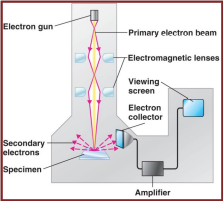
Scanning electron microscopes use an electron beam to illuminate a sample. The electrons are scattered by the interactions with the atoms in the sample. In Scanning Electron Microscopy (SEM) backscattered electrons (BSE) are used to create an image. These electrons originate from the area just below the surface and provide compositional information of the sample.

Alternatively, secondary electrons can be measured. This type of electrons is released from the surface by inelastic interactions of the primary electron beam and the sample. Secondary electrons have lower energy and can be analysed separately from BSEs. Whereas BSEs originate from the area somewhat below the surface of the sample, secondary electrons provide topographical information of the surface area.

Apart from electrons, the interaction of the electron beam with the sample can also produce energy-dispersive X-rays (EDS). These X-rays are characteristic for the atom in which they are generated. Thus, an EDS spectrum contains information on the elements of which the sample is composed.


Instead of visual optics, all forms of electron microscopy use electromagnetic lenses, both to focus the electron beam and to create the image by removing aberrations. The electrons in the beam are accelerated. A higher acceleration voltage results in a higher resolution, but it may damage fragile samples like biological samples or very thin samples, like graphene. By using different techniques, our microscopes can combine low voltage with high resolution.

Interactions between the primary electron beam and the surface of the sample.
General configuration within SEM instruments.

Why use a Scanning Electron Microscope?

Scanning Electron Microscopy allows you to see the smallest structures, even up to atomic resolution. ST Instruments offers solutions to make sub nanometre details visible. For the study of surfaces, SEM is the preferred method. The technique allows you to see a large part of your sample at low magnification and zoom in to study details at high magnification. Through EDS spectra, the composition can be analyzed. SEM’s are available in a range of desktop SEMs to top-of-the-line systems, tungsten, Schottky, cold field and prices are completely dependent on  the system configuration.

How much does a Scanning Electron Microscope cost?

Scanning Electron Microscopes are available in a range of desktop SEM’s to top-of-the-line systems, tungsten, Schottky, cold field and prices are completely dependent on the system configuration.

Applications for Scanning Electron Microscopy

SEM / TEM asbestos fiber analysis

In the past, asbestos was commonly used as building material because of its strong mechanical qualities and thermal insulating properties. Research demonstrated that asbestos can cause serious health issues and for that reason, this mineral was banned from construction sites in the mid-nineties. Many building materials are tested for asbestos to ensure a safe working environment. SEMs and TEMs equipped with EDS are deployed to analyse and detect the microscopic asbestos fibres.

SEM nanoparticle analysis

Nanoparticle analysis is a common field of interest in many disciplines such as material science, life science and semiconductor industry. With a Scaning Electron Micoroscope it is possible to obtain high-resolution images of individual nanoparticles and observe the surface. In addition, particle distribution characterization and counting are available.

Sample preparation

Many samples are cut and polished before SEM imaging. For optimal surface or cross-section analysis an ion-miller is beneficial. An ion-beam ejects atoms from the surface of a sample without mechanical stress. This leaves a perfectly polished surface, which is ideal for many damage-sensitive materials.

SEM image of asbestos fibers.
SEM visualization of gold nanoparticles (left).
Traditional mechanical polishing (left)
The elemental composition of these particle is confirmed by EDX (right).
Ion milling (right)