Table Of Contents
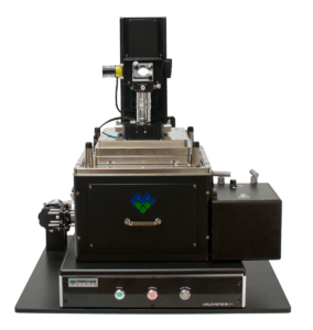
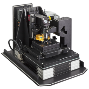
How does AFM-IR/PiFM work?
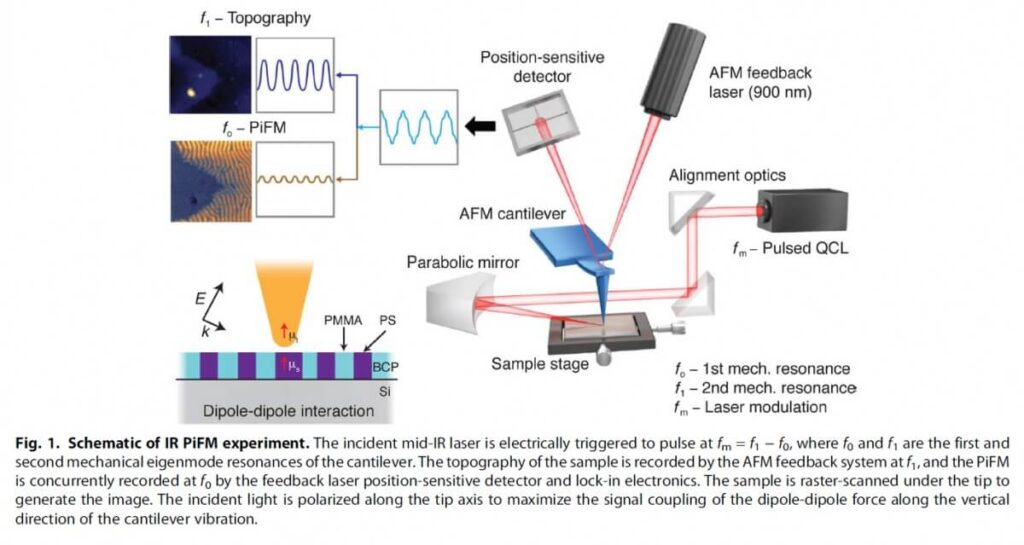
In AFM-IR or nanoIR, the atomic force tip scans the sample while an infrared laser excites the sample to facilitate IR spectroscopy. Thus, both the topography and the chemical spectra are recorded with high resolution. There are several ways to measure the IR absorption spectra through the AFM tip. In PiFM, the photoinduced force is the result of a dipole-dipole force attraction between the imaging tip and the sample when illuminated with a monochromatic, coherent light source.
Through imaging at multiple IR wavelengths, corresponding to absorption peaks of different chemical species, PiFM has the ability to spatially map nanometre-scale patterns of the individual chemical components. A schematic diagram of PiFM is shown below:
Why use AFM-IR/PiFM?
Compared to competing AFM-IR techniques, photo-induced force microscopy has several advantages. For example, in photo-thermal AFM-based techniques, the thermal expansion in the sample can reduce the spatial resolution and surface sensitivity. For scattering SNOM type AFM-IR techniques the spatial resolution and surface sensitivity are good but important challenges remain in the interpretation of the images, the extraction of useful information from the background and the presence of artefacts in the optical image.
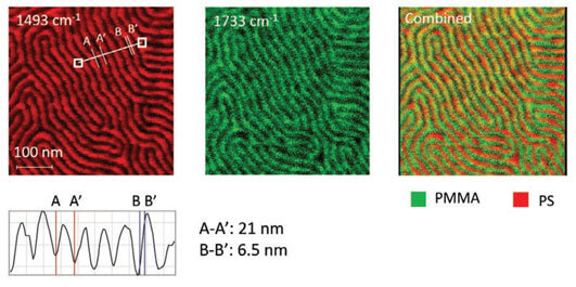
PiFM has an excellent signal to noise ratio and a small interaction volume, leading to increased spatial resolution. It is for example possible to resolve the different chemical blocks of a PS-b-PMMA block copolymer sample with a pitch of about 22 nm (the rise of the signal / resolution measures less than 7 nm).
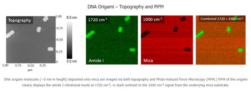
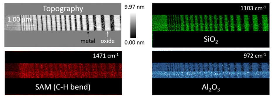
Excellent surface sensitivity is demonstrated in the DNA origami measurement below. Especially the image at 1000 cm-1 which highlights Mica shows that the technique does not measure the Mica under the 3nm DNA patch.
Finally, PiFM does not suffer from background interference and shows a good correlation with conventional IR-spectra from bulk materials without sample thickness effects.

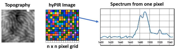
A powerful way to analyse unknown samples is hyperspectral AFM-IR imaging (hyPIR), providing images of all the resonant modes in a structure with a single scan. A 128 by 128 pixel grid can be produced in about one hour.
PiFM examples
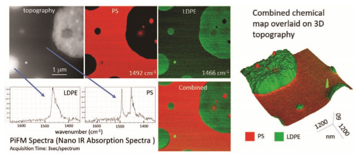
Using Infrared photo-induced force microscopy you will be able to acquire IR spectra while simultaneously mapping topography. Infrared wavelengths specific to different chemical entities resolve the nanometre-scale distribution of each chemical species in diverse multi-phase and multi-component systems.
For example, hyperspectral infrared PiFM will give you a quick idea about the chemical makeup of perovskite photovoltaic films, which have a complicated domain structure. The scan shows different chemical phases and chemical transitions across phase boundaries.
DNA origami molecules (~3 nanometre in height) deposited onto mica are readily imaged via both topography and PiFM. The signal of the DNA molecules clearly shows the amide I vibrational mode.
For many semiconductor applications, PiFM is a viable tool for, amongst others, the visualization and analysis of area selective deposition (ASD / Image below), local strain, the cross-section of a trench, the cross-section of a multilayer stack, chemical mechanical polishing (CMP), buried conductive layers and defect analysis.
As the future of materials science is nano, photo-induced force microscopy (AFM-IR) is an indispensable tool to analyse the topology and chemical makeup of new materials in exquisite detail.
Atomic Force Microscopy
Atomic Force Microscopy makes it possible to create images based on topological information at sub-nanometer resolution (topological imaging). However, the interaction of the tip with the surface also allows measurement of mechanical properties (force measurement), electrical, thermal and magnetic properties. Finally, the tip can also be used to manipulate a sample in a controlled way at the nanometer level.
How does Atomic Force Microscopy work?
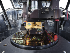
The AFM tip is attached to the free end of a cantilever. Cantilever and tip together are usually referred to as the AFM probe. When the tip is passed over the surface of a sample, upwards movement and deflection of the tip is measured using laser light reflected via the cantilever onto a position-sensitive photo diode. The sample is moved during scanning, and movement is controlled by piezoelectric elements.
To create images, the tip is in (near) contact with the sample. When it is approaching the surface, attractive forces dominate, causing the cantilever to bend towards it. As the tip makes contact, however, repulsive forces begin to dominate, bending the cantilever upwards. This deflection of the cantilever is measured and recorded. A feedback loop is used to keep the force between the probe tip and the surface constant. The result is a topographical map of the surface. The settings of the feedback affect the noise, and thus the image quality.
Imaging is just one application of Atomic Force Microscopy. Different modes are available to measure different interactions between the probe and the sample.

Why use Atomic Force Microscopy?
The major application for an atomic force microscope is imaging sample topography in high resolution. The challenge for high resolution imaging lies in the capability of the specific instrument to keep the AFM tip sharp. There are several different imaging modes available:
- True non-contact mode: The benefits of non-contact mode atomic force microscopy are well established: no tip wear, no sample damage, maintenance of high resolution imaging, and high accuracy of AFM measurement. In True Non-Contact™ mode, the tip-sample distance is successfully maintained at a few nanometers in the net attractive regime of inter-atomic force between tip and sample. The small amplitude of tip oscillation minimizes the tip-sample interaction, resulting in superb tip preservation and negligible sample modification.
- Contact mode: In contact mode, also known as repulsive mode, an AFM tip makes soft physical contact with a sample. This is the preferred technique for some electrical modes, even though it is not an ideal mode for imaging since there is higher tip wear. It is not an ideal mode for imaging since there is higher tip wear but for some electrical modes it is one of the preferred techniques.
- Tapping mode: Unlike non-contact mode, this mode uses higher amplitude of tip oscillation and works in both the repulsive- and attractive regime. The tip-sample interaction is larger which results in faster degradation of the tip.
Apart from creating images, Atomic Force Microscopy allows you to characterize a wide array of properties based on the interaction of the probe with the sample. e.g. mechanical, electrical, magnetic or optical. AFM probes can also be used to manipulate the sample, for example for lithography or to perform experiments through molecular pulling. Thus, Atomic Force Microscopy allows you to probe the properties of a surface on nanoscale.

Applications of Atomic Force Microscopy
Electrical and Mechanical Characterization of Li Ion Battery Electrode
Lithium ion batteries are powering most of our modern electronics. To further improve their performance, it is vital to understand the electrical and mechanical properties of electrode materials, preferably at nanometre scale.
One of the more effective tools used to measure electrical properties of these electrodes on this small scale is Scanning Spreading Resistance Microscopy (SSRM). This technique, which is based on Atomic Force Microscopy, simultaneously measures both electrical properties and topography. However, SSRM has some disadvantages such as rapid wearing of the tip though contact with the sample and low signal-to-noise ratio.
Park Systems recently developed an Atomic Force Microscopy mode which performs SSRM in an approach-retract manner (PinPoint SSRM) which eliminates tip-sample contact, while still providing excellent electrical properties measurements as well as acquiring topography. The system allows an overlay of different measurements, like topography, resistance and conductance, to provide detailed insight into the properties of the batteries. This will help engineers to understand their electrical and mechanical properties.

Defect Recognition on Coating Layer
As Atomic Force Microscopy measures both surface morphology and mechanical properties, it is an excellent technique for a review and inspection of quality control for possible defects in coated surfaces. For example, it can distinguish a scratch made on a glass surface before coating from a scratch after coating. In the latter case, the glass will be exposed.
The PinPoint™ nanomechanical mode which Park Instruments developed for the Atomic Force Microscope collects high resolution topographical data while simultaneously obtaining force-distance data. This allows simultaneous measurement of the surface morphology and nanomechanical properties including modulus, adhesion, deformation, stiffness and energy dissipation.
Topographical data will show a similar pattern in a scratch made before or after coating. Furthermore, in a sample that was scratched before coating all the material will have the same mechanical properties. However, in a sample scratched after coating, the exposed glass will stand out against the coating because of its different mechanical properties. This type of information will help to identify problems in the production process.
Optimum Current Distribution Measurement of Zinc Oxide Nanorods
In ever smaller electrical devices, it is increasingly difficult to measure the current distribution in the material they are made of, which is an important parameter in determining the performance of devices. Conductive Atomic Force Microscopy (C-AFM) provides both electrical properties and topography at the same time and at nanoscale. However, this method has its drawbacks like quick tip wear from high frictional force due to continuous tip-sample contact and high signal-to-noise ratio.
PinPoint™ is an operational Atomic Force Microscopy mode developed by Park Systems that can be coupled with C-AFM to offer an innovative solution to these problems. This method operates in an approach-retract manner, ensuring a frictionless operation. Studies on ZnO nanorods, which show a remarkable performance in electronics, optics, photonics, and photocatalysis, shows this new method is superior to either C-AFM or tapping AFM.
One advantage of the PinPoint™ Atomic Force Microscopy mode is that contact time and contact force between the tip and sample surface are controllable (as opposed to the standard tapping mode), allowing acquisition of accurate and reproducible data even with soft samples, such as polymers.
