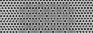
The study is based on the optical properties of QDs that are embedded in PhC cavities (Figure 1a), leading to enhanced emission (the Purcell effect), or in WGs (Figure 1b), producing photon multiplexing devices. A typical device is fabricated from a multi-layer GaAs/Al0.7Ga0.3As/GaAs epitaxially grown stack, where the top 250 nm thick GaAs layer contains the active part of the device, and the 1 μm Al0.7Ga0.3As sacrificial layer is eventually etched away to produce a floating membrane device (Figure 1c). This membrane contains one or several 20 nm In0.3Ga0.7As QDs in specific positions, and an etched PhC structure (large array of 100 nm holes, with several holes missing in a specific configuration), precisely aligned with the QDs. These devices require accuracies of 1-20 nm in several processing steps, so they all involve high-performance electron-beam lithography and plasma (ICP) etching. The crucial final step is the membrane release, involving wet etching of the sacrificial layer. Since at this stage there is no possibility to look at a cross-section of the samples, top-view Optical Microscopy and Scanning Electron Microscopy (SEM) are the only possible tools to characterize the PhC structures.
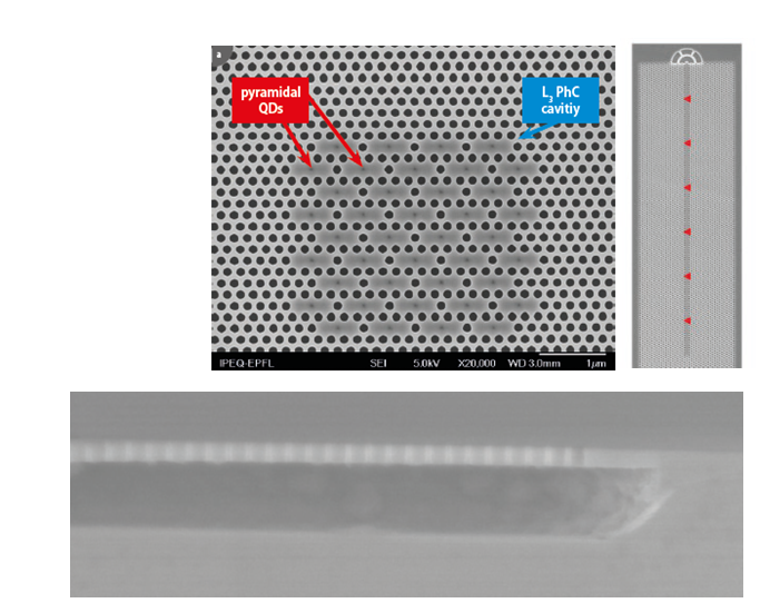
Figure [1] a) SEM image of a network of QDs (darker spots) embedded in coupled L3PhC cavities. b) SEM image of PhC waveguide with an out-coupler at the top, containing six QDs (indicated by red triangles). c) SEM cross-section image of the suspended membrane device
In this study, the S neox was used. The S neox provides up to 4 different light sources (red, green, blue and white), which is particularly relevant in this study as the use of 2D brightfield high-magnification imaging with a red light source enables us to probe the features under the membrane hat are otherwise invisible. The purpose of this study is the high-precision (sub-μm) non-destructive characterization of photonic crystal devices fabricated on thin (250 nm) suspended GaAs membranes.
Measurements
We observed the floating membrane devices by brightfield microscopy, using the 150X objective (sometimes combined with further image zoom), using the microscope’s four LED light sources. As a first approximation, we always suppose that the observed image reflects the surface feature of the device. However, in some devices, e.g. those containing dielectric layers, light can penetrate the top layer and provide information about the inner parts, which is extremely useful. Therefore, we tried to apply this technique to our floating membrane devices. As is well known, GaAs is opaque at the visible spectral range, due to its gap energy of 1.52 eV (815 nm) at room temperature.
At all shorter wavelengths, the absorption coefficient of GaAs is large and strongly wavelength-dependent:1 it varies by a factor of 5 between the red LED (3.9μm-1 at 630 nm) and the blue LED (20.4μm-1 at 460 nm) used in the Sensofar microscope. However, for the thin membranes (250-260 nm) that we use, there is a good chance of recovering useful information from the bottom part of the device, at least with red light, which is less absorbed by the membrane.
In Figure2a-d we see brightfield images (taken with 150x objective plus x4 zoom) of a PhC membrane device, depicted as a gray hexagon, as individual 100 nm holes cannot be imaged. We show images taken with the red (2a), green (2b), blue (2c), white (2d) LEDs. We can clearly observe the effect of the LED wavelength on the image: While the blue image (Figure2c) shows only the top part of the device, the red image (Figure 2a) shows features beyond the device edges, showing as a dark band. These features correspond to the under-etched regions of the device, which are observed through the membrane when using red light. The green (Figure 2b) and white (Figure 2d) images show very weak features of the underetched zone, as we expect from the spectra in Figure 3. We also see that the central part (PhC zone) is brighter than the background in red light (2a) and darker in all other lights (2b-d). This could be an interference effect related to the membrane thickness. Another aspect is of course the higher resolution of the blue images (Figure 2c,f ) compared to the red ones (Figure 2a,e), as can be observed in the smaller images of the sub-micron (0.4×0.8 μm) cavity at the center of the device. Finally, in Figure 2e,f we show the same devices in dark-field, using red and blue LEDs, respectively. The edges of the undercut zone (Figure 2e) and of the top of the device (Figure 2f ) are clearly seen. In both images we also observe some granularity, which we can thus deduce to be on the surface of the device and not underneath.
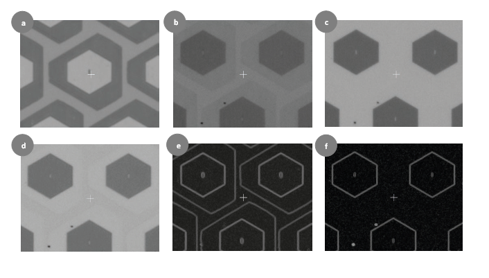
Figure [2]. Brightfield images of a PhC cavity device, all taken using the x150 objective (Brightfield, zoom x4). Light source is Red LED (a). Green LED (b), Blue LED (c) and White LED (d). In (e) and (f) we see the dark-field images taken with Red and Blue LEDs, respectively (corresponding to the BF images in a and c)
Go to ‘request application note’ and download the full application note.