Overcome charge-up effects in Scanning Electron Microscopes (SEMs)
during non-conductive specimen observation with Hitachi’s Ultra-Variable pressure Detector (UVD)
during non-conductive specimen observation with Hitachi’s Ultra-Variable pressure Detector (UVD)
A Scanning Electron Microscope (SEM) scans a sample surface with a converged electron beam. At high specimen chamber pressure, electrons from this beam hit gas molecules and the mean free path of the electrons becomes shorter. This negatively influences image quality. Hence, high-vacuum levels are generally desired. In case of non-conductive samples however, charge-up effects could occur. One way to deal with these effects is to apply a low-vacuum in the specimen chamber of the SEM. Downside of this strategy is that secondary electrons, typically having small amount of energy, collide with gas molecules too and don’t arrive at a general detector. This application note describes the innovative solution from Hitachi to acquire topographic information in SEMs, originating from secondary electrons, while charge-up effects are avoided.
Charge-up is an undesirable effect in SEMs where the negative charge of the incident electron beam accumulates on the surface of a non-conductive specimen. This occurs when the total number of electrons emitted from a sample, the sum of backscattered electrons, secondary electrons and absorbed electrons, is less than the incident electrons. The potential on the specimen surface becomes negative and causes various distortions in secondary electron imaging.

Image 1. Examples of charge-up effects
Sample coating circumvents this problem by allowing the charge on the specimen surface to flow away. However, coating of the sample has some disadvantages. The film layer impairs with the specimen surface characteristics and influences elemental composition measurements. An alternative to this additional processing step is SEM imaging in a low vacuum chamber, the so-called charge-up reduction (Variable Pressure) mode. Electrons from the beam collide with the gas molecules in the chamber, leaving positive ions which are attracted to the redundant electrons on the specimen surface. In this way excess electrons on the surface are neutralized and charge-up effects are eliminated, as depicted in image 2.

Image 2. Charge-up effects are reduced by operating the SEM in low-vacuum environment.
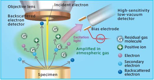
In comparison to backscattered electrons, secondary electrons have only a low amount of energy. Therefore, secondary electrons have not enough energy to travel through the gaseous environment. This makes it impossible to create clear SE images. To overcome this issue, Hitachi developed an Ultra-Variable pressure Detector (UVD). As secondary electrons hit gas molecules, photons are released which are subsequently attracted to the UVD by a high voltage. These signals are then converted to topographic images, enabling a clear observation of the specimen’s surface. Image 3 visualizes the working principle behind this technique.

Image 3. Schematic diagram showing the working principle of Hitachi’s Ultra-Variable pressure Detector (UVD) to eliminate charge-up effects and to obtain topographic information of non-conductive samples.
Utilizing the UVD from Hitachi, charge-up effects are suppressed in a low vacuum SEM without sputtering a conductive film to allow observation of non-conductive specimens. This is an ideal solution for SEMs which are already operating at low vacuum, like the TM4000Plus table top SEM. However, the Ultra Variable pressure Detector is also available on other high-end SEMs from Hitachi, such as the SU3900 for handling large and heavy samples.