
Introduction
Radio frequency (RF) and power electronics are vital to an array of industries, from telecom and consumer electronics to transportation and energy distribution. As energy diversification and the prevalence of high-speed electronics continue to grow, RF and power electronics are expected to reach a global market of $36.6 billion by 2027.[1] Extreme environments such as high temperatures, ultra-violet radiation, oxygen, salinity, and moisture are all threats that degrade and corrode active components causing early failure.
Atomic Layer Deposition (ALD) has created substantial improvements to the reliability and performance of RF and power electronics. Using ALD as an encapsulation layer at the wafer level or as a final hermetic seal at the chip/module/PCB level has been shown to substantially improve electronic performance and lifetime.[2][3] ALD Layers enable longer lifetimes, higher performance and lower cost without adding considerable mass gain and high temperature processing associated with conventional hermetic coatings.
ALD improves RF an Power Electronics
The benefits of ALD layers:
- Hermetic sealing encapsulation layers with minimal thickness
- Pristine conformality in high-aspect ratio structures
- Ultra-low particle generation
- Low stress films
- Improved lifetime of ICs and PCBs
- Increased resistance to harsh environments
- No peeling or flaking of the hermetic seal at pressure >1200 PSI
- Negligible mass gain from coating at 100 nm
There are two major methods of using ALD in RF and power electronics:
1. Overcoat encapsulation at the wafer level
2. Hermetic sealing at the package level
ALD at the Wafer Level
One of the most important layers in post-gate processing for RF and power devices is the encapsulation layer to protect the device from environmental degradation. This encapsulation layers have found to decrease humidity permeation rates on moisture sensitive devices.[4] In a study from April 2020, RF microelectronic mechanical devices (MEMs) were encapsulated with SiNx thin films for environmental protection on 5G devices and showed successful mechanical protection.[5] Beyond environmental protection, encapsulation layers have also been found to improve RF device performance. One study showed encapsulated GaAs-based terahertz emitters increase the average power output fourfold by enhancing the conductivity and prevention oxidation at the semiconductor surface. [6]
Plasma enhanced chemical vapor deposition (PECVD) has historically been used for encapsulation deposition, however, the use of plasma damages delicate semiconductor surface states with energetic ions, chemical radicals and UV radiation. Presence of these surface states gives rise to hopping conduction, which lowers the breakdown voltage of the gate. The thermal nature of ALD does not require damaging plasma or high energy ions for deposition and helps maintain delicate surface electronic states and increases reliability of the circuit.[2]
ALD provides an electrically-low-leakage film, with no pinholes and a high dielectric constant at deposition temperatures down to 80°C. With these improvements in film quality, ALD has largely started to displace PECVD in post-gate processing as deposition rates have increased.[10] Common ALD chemistries for this application, such as Si3N4, Al2O3, HfO2, TiO2 and ZnO can be deposited b ALD using commercial precursors commonly used for PECVD/CVD processes.[2]
Compared to other deposition techniques ALD provides a hermetic seal which provides greater device protection. Sputtering, physical vapor deposition (PVD), and CVD provide imperfect coatings where pinhole defects are common. These pinholes defects provide point locations for corrosion to enter the device leading to early failure.[7] the low-stress and pinhole-free ALD films provide a vital protective barrier over the active device. Active devices will fail if moisture finds a path to the ohmic contacts, channels of field effect transistors (FETs), or junctions of heterojunction bipolar transistors (HBTs). However, these active devices are well-protected from moisture with ALD films. In one study, SiN ALD encapsulated FETs were compared with PECVD encapsulated FETs under an accelerated stress test, 130° and 85% relative humidity, the PECVD coated FETs had a 99% failure rate compared to 2.7% for ALD coated FETs, predicting reliable ALD performance under worst-case conditions for MMICs.[8]
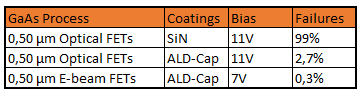
Table 1: A 96 hour Highly accelerated stress Test (HAST) at 130°C and 85% relative humidity was used as a benchmark for the optimization of the ALD layers. The devices are biased at pinchoff during the test which is the maximum stress condition. The ALD FETs had a much lower failure rate than the original SiN FETs.[8]
Learn More?
Please click on ‘Request Application Note’ and we will send you the full application note ‘Atomic Layer Deposition for Encapsulation and Hermetic Sealing of RF and Power Electronics’.