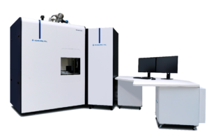
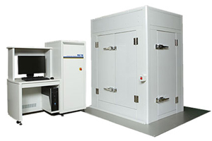
Techniques
Surface analysis techniques like XPS (X-ray Photoelectron Spectroscopy), TOF-SIMS (Time-of-Flight Secondary Ion Mass Spectrometry), and AES (Auger Electron Spectroscopy) are essential tools for investigating the composition and chemistry of materials at the atomic and molecular level. Each technique offers unique capabilities for characterizing surfaces, interfaces, and thin films:
- XPS (X-ray Photoelectron Spectroscopy): XPS is a non-destructive technique that provides valuable information about the elemental composition and chemical states of a material’s surface. It operates by irradiating the sample with X-rays, causing electrons to be ejected from the inner core levels of the atoms. The energy of these emitted photoelectrons is measured, allowing researchers to identify the elements present and their chemical environments. XPS is highly surface-sensitive, offering information about the outermost layers of a sample. It is commonly used for depth profiling, analyzing surface contamination, identifying oxidation states, and characterizing the binding energies of atoms. XPS is applicable to a wide range of materials, including metals, semiconductors, polymers, and biomaterials.
- TOF-SIMS (Time-of-Flight Secondary Ion Mass Spectrometry): TOF-SIMS is a technique that excels in providing chemical information about the surfaces of materials with high spatial resolution. It involves bombarding the sample surface with a primary ion beam, which leads to the emission of secondary ions from the surface. These ions are analyzed based on their time-of-flight to a detector, allowing for the determination of their mass-to-charge ratios. TOF-SIMS offers both elemental and molecular information, enabling the identification of specific compounds and functional groups on the surface. It is particularly useful for chemical mapping, depth profiling, and analyzing organic and inorganic materials. TOF-SIMS finds applications in fields like semiconductor manufacturing, biomaterials research, and materials science.
- AES (Auger Electron Spectroscopy): AES is a surface-sensitive technique that involves the analysis of Auger electrons emitted when atoms in a material transition to lower energy states. It provides information about the elemental composition and chemical bonding of the top few atomic layers of a sample. AES is highly useful for identifying elements, studying chemical shifts, and investigating chemical reactions at surfaces. It is particularly sensitive to surface contamination, adsorbates, and thin films. AES can be used to characterize the composition of metals, semiconductors, ceramics, and insulating materials. It can also offer depth profiling capabilities by gradually removing material through ion sputtering.
In summary, XPS, TOF-SIMS, and AES are powerful surface analysis techniques that provide complementary information about the composition and chemistry of materials at the atomic and molecular scale. Researchers choose these techniques based on their specific analytical needs, the depth of information required, and the type of material being studied. These techniques play a crucial role in advancing fields such as materials science, nanotechnology, electronics, and biomedicine by enabling precise characterization of surfaces and interfaces.