Plasma Etching


Plasma etching is a process that uses ionised gas (plasma) to selectively remove material, clean surfaces, or modify surface properties. One of the most common forms of plasma etching is Reactive Ion Etching (RIE), which uses reactive plasma chemistry to achieve controlled, repeatable material processing.
Plasma etching is widely used in semiconductor research, nanotechnology, and advanced materials development to create device structures, transfer patterns, prepare surfaces, and optimise material performance. By selecting the appropriate process gases and operating conditions, researchers can perform everything from gentle surface activation and cleaning to highly controlled etching of materials such as graphene, h-BN, silicon, and silicon dioxide.
The ability to precisely control etch rates, surface modification, and material removal makes plasma etching a key technology for applications including 2D materials research, semiconductor device fabrication, nanostructure development, photonics, MEMS, and advanced sensor technologies.
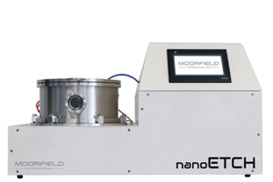
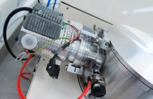
soft plasma etching

♦   nanoETCH | Modular Plasma Etching System

How does Plasma Etching work?

Plasma etching is a process that uses ionised gas (plasma) to selectively remove material, clean surfaces, or modify surface properties. The process takes place in a vacuum chamber, where process gases are energised to create a plasma containing reactive species that interact with the surface of the material being processed.


By carefully controlling process parameters such as gas chemistry, pressure, power, and treatment time, plasma etching can be used for a wide range of applications, from gentle surface cleaning and activation to precise material removal and pattern transfer. Different plasma chemistries can be selected to target specific materials, enabling controlled and repeatable processing for research and development applications.


Plasma etching is widely used in semiconductor research, nanotechnology, photonics, MEMS fabrication, and advanced materials development. Typical applications include etching silicon and silicon dioxide, processing graphene and other 2D materials, surface activation, plasma cleaning, and the fabrication of nanoscale devices and structures.


The ability to achieve precise, repeatable material processing while maintaining excellent control over surface properties makes plasma etching an essential technology for modern microfabrication and advanced materials research.

Why use Plasma Etching?

Plasma etching is widely used in research and development because it provides a highly controlled method for material removal, surface modification, and substrate preparation. By selecting the appropriate process gases and operating conditions, researchers can tailor the process to achieve precise and repeatable results across a wide range of materials and applications.


One of the key advantages of plasma etching is its versatility. The technology can be used for semiconductor processing, graphene and 2D materials research, thin-film patterning, plasma cleaning, and surface activation. This flexibility allows researchers to perform multiple processes within a single platform while maintaining excellent control over etch rates and surface properties.


Plasma etching also supports the fabrication of advanced devices and nanostructures, making it an essential tool in nanotechnology, photonics, MEMS development, sensor fabrication, and microelectronics research. Its ability to deliver reproducible results and application-specific process control makes plasma etching a valuable technique for both fundamental research and technology development.

Applications of Plasma Etching

Plasma etching is widely used across semiconductor research, nanotechnology, advanced materials development, and microfabrication. Its ability to provide controlled material removal, surface modification, and plasma cleaning makes it a versatile process for a broad range of applications.


Graphene & 2D Materials Processing

Plasma etching enables the controlled patterning, cleaning, and modification of graphene, h-BN, transition metal dichalcogenides (TMDs), and other 2D materials while preserving critical material properties.


Semiconductor & Microelectronics Research

Reactive ion etching (RIE) is widely used for the fabrication of semiconductor devices, thin-film structures, and microelectronic components, providing precise and repeatable material processing.


MEMS & Microsystems Fabrication

Plasma etching supports the development of micro-electromechanical systems (MEMS) by enabling the creation of complex microstructures and high-precision device features.


Photonics & Optoelectronics

The technology is used to fabricate waveguides, optical coatings, photonic devices, and optoelectronic components where accurate feature definition and surface quality are essential.


Surface Cleaning & Activation

Argon and oxygen plasma processes can be used to remove surface contamination, improve adhesion, activate surfaces, and prepare substrates for deposition, bonding, or further processing.


Nanotechnology & Advanced Materials Research

Plasma etching is a key enabling technology for nanoscale device fabrication, nanostructure development, sensor research, and the investigation of emerging materials and coatings.


The flexibility of plasma etching allows researchers to tailor process parameters and gas chemistries to meet specific application requirements, making it an essential tool for both fundamental research and technology development.