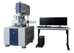
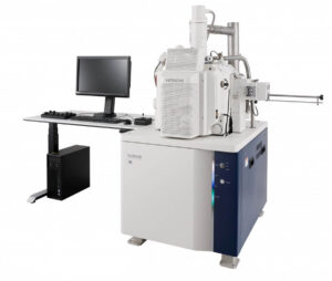
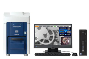
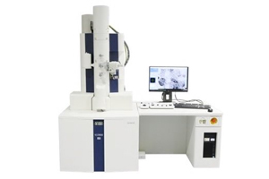
♦ SU8600 | High-brightness cold field emission source provides ultrahigh-resolution images even at Ultra-low voltages
♦ SU9000 | Features the world’s highest SE resolution of 0.4 nm at 30 kV
♦ SU8700 | Characterized by its Ultrahigh-Resolution and Analytical Capability
♦ SU7000 | Characterized by its versatile imaging capacity
♦ SU5000 | With revolutionary computer-assisted EM Wizard technology
♦ SU3800 | VP-SEM with thermionic electron source
♦ SU3900 | VP-SEM with thermionic electron source and large sample chamber
♦ TM4000Plus II | With a high-sensitivity low-vacuum SE detector
♦ TM4000 II | Integrates ease of use, optimized imaging, and high-image quality
♦ FlexSEM 1000 II | Compact variable-pressure SEM with unparalleled image resolution
♦ ArBlade 5000 | Cross-section widths up to 8 mm
♦ IM4000II | Dual milling configuration in a single instrument
♦ ZONESEM II | Tabletop Specimen Cleaner
♦ ZONETEM II | Sample Cleaner
Scanning electron microscopes use an electron beam to illuminate a sample. The electrons are scattered by the interactions with the atoms in the sample. In Scanning Electron Microscopy (SEM) backscattered electrons (BSE) are used to create an image. These electrons originate from the area just below the surface and provide compositional information of the sample.
Alternatively, secondary electrons can be measured. This type of electrons is released from the surface by inelastic interactions of the primary electron beam and the sample. Secondary electrons have lower energy and can be analysed separately from BSEs. Whereas BSEs originate from the area somewhat below the surface of the sample, secondary electrons provide topographical information of the surface area.
Apart from electrons, the interaction of the electron beam with the sample can also produce energy-dispersive X-rays (EDS). These X-rays are characteristic for the atom in which they are generated. Thus, an EDS spectrum contains information on the elements of which the sample is composed.
Instead of visual optics, all forms of electron microscopy use electromagnetic lenses, both to focus the electron beam and to create the image by removing aberrations. The electrons in the beam are accelerated. A higher acceleration voltage results in a higher resolution, but it may damage fragile samples like biological samples or very thin samples, like graphene. By using different techniques, our microscopes can combine low voltage with high resolution.
Scanning Electron Microscopy allows you to see the smallest structures, even up to atomic resolution. ST Instruments offers solutions to make sub nanometre details visible. For the study of surfaces, SEM is the preferred method. The technique allows you to see a large part of your sample at low magnification and zoom in to study details at high magnification. Through EDS spectra, the composition can be analyzed.
SEM / TEM asbestos fiber analysis
In the past, asbestos was commonly used as building material because of its strong mechanical qualities and thermal insulating properties. Research demonstrated that asbestos can cause serious health issues and for that reason, this mineral was banned from construction sites in the mid-nineties. Many building materials are tested for asbestos to ensure a safe working environment. SEMs and TEMs equipped with EDS are deployed to analyse and detect the microscopic asbestos fibres.
SEM nanoparticle analysis
Nanoparticle analysis is a common field of interest in many disciplines such as material science, life science and semiconductor industry. With SEM it is possible to obtain high-resolution images of individual nanoparticles and observe the surface. In addition, particle distribution characterization and counting are available.
Sample preparation
Many samples are cut and polished before SEM imaging. For optimal surface or cross-section analysis an ion-miller is beneficial. An ion-beam ejects atoms from the surface of a sample without mechanical stress. This leaves a perfectly polished surface, which is ideal for many damage-sensitive materials.