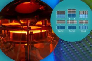
Thermal Processing/ Annealing


Annealing is a heat treatment process used in materials science and metallurgy to modify the properties of a material, typically a metal or an alloy. The main objective of annealing is to alter the microstructure of the material to achieve specific characteristics, such as increased ductility, improved hardness, reduced brittleness, or relief from internal stresses. Annealing is a controlled heating and cooling process that can be applied to a variety of materials for different purposes.

♦   Anneal | Thermal treatment of 2D measurements

How does Thermal Processing/ Annealing work?

Annealing is a heat treatment process that works by changing the microstructure of a material, often a metal or alloy, to achieve specific material properties. The process involves controlled heating and cooling, and how it works can vary depending on the type of annealing being used.


  1. Heating: The material to be annealed is heated to a specific temperature. The choice of temperature is crucial and depends on the material’s composition and the desired outcome of the annealing process. Typically, the material is heated above its recrystallization temperature or above a critical point.
  2. Soaking: Once the material reaches the target temperature, it is held at that temperature for a specified period. This soaking time allows the internal structure of the material to transform. During this stage, several important processes can occur:
  • Recovery: The material begins to recover from prior deformation or stresses. Some of the dislocations (structural defects) in the material annihilate or rearrange, reducing internal stress.
  • Recrystallization: In processes like full annealing or recrystallization annealing, new grains can form in the material. This process involves the creation of new, defect-free grains, which results in increased ductility and improved mechanical properties.
  • Phase Transformation: In some materials, annealing can induce phase transformations, changing the material’s crystal structure and properties.
  1. Cooling: After the soaking period, the material is cooled down. The cooling rate and method can vary depending on the desired outcome:
  • Full Annealing: In full annealing, the material is cooled slowly in a controlled manner, often in the furnace or air, to room temperature. This slow cooling allows the microstructure to stabilize and minimize internal stresses.
  • Process Annealing: Process annealing involves slow cooling as well but is typically done at a lower temperature to reduce hardness and restore ductility in cold-worked materials.
  • Quenching: Some annealing processes, especially in hardening applications, involve rapid cooling (quenching) to “lock in” the new microstructure created during the heating phase.


The specific parameters of the annealing process, including the heating temperature, soaking time, and cooling rate, are tailored to the material’s composition, its initial state, and the desired material properties. Annealing can be used to achieve a range of outcomes, such as improved ductility, reduced hardness, stress relief, and changes in the material’s microstructure. It is a crucial technique in metallurgy, materials science, and manufacturing to optimize the performance of materials in various applications.

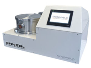
Why would you use Annealing?

Annealing in semiconductors is a crucial process used to modify the properties of semiconductor materials, repair defects, and activate dopants. The specific mechanisms of annealing in semiconductors can vary depending on the type of annealing process and the desired outcome. Some typical applications where thermal processing / annealing is applied:


  1. Dopant Activation:
  • Process: When dopant atoms, which are introduced by ion implantation or diffusion, are embedded into the semiconductor crystal lattice, they are often in an electrically inactive state. Annealing is used to activate these dopants by allowing them to move within the crystal lattice, become substitutional (replace silicon atoms in the lattice), and contribute to the desired electrical properties.
  • Mechanism: Annealing provides thermal energy that allows the dopant atoms to overcome energy barriers and settle into substitutional sites within the lattice. The temperature and duration of the annealing process are carefully controlled to ensure effective activation while minimizing damage or defects.
  1. Defect Repair:
  • Process: Annealing can repair crystal lattice defects or damage introduced by ion implantation or other processes. This is particularly important for maintaining the structural integrity and electrical performance of semiconductor materials.
  • Mechanism: During annealing, vacancies and interstitials in the crystal lattice are mobile, and they can migrate and recombine to reduce defects. The thermal energy provided by annealing facilitates the mobility of these defects.
  1. Amorphous to Polycrystalline Transformation:
  • Process: Annealing is used to transform amorphous silicon (a-Si) into polycrystalline silicon (poly-Si) in some applications, such as thin-film transistors (TFTs).
  • Mechanism: Annealing at elevated temperatures induces crystallization of the amorphous silicon, leading to the growth of polycrystalline grains. The annealing process allows the silicon atoms to reorganize and form a regular crystal structure.
  1. Oxidation and Nitridation:
  • Process: Annealing can be used to grow silicon dioxide (SiO2) or silicon nitride (Si3N4) layers on silicon wafers, which are essential insulating materials in semiconductor devices.
  • Mechanism: During annealing, silicon wafers are exposed to oxygen or nitrogen, and the high temperature facilitates the chemical reaction between the silicon and these gases, leading to the formation of the desired insulating layers.
  1. Diffusion and Junction Formation:
  • Process: Annealing is used to facilitate the diffusion of dopant atoms in the semiconductor, creating controlled junctions in devices like transistors.
  • Mechanism: Annealing at specific temperatures promotes the movement of dopant atoms within the semiconductor lattice, allowing them to distribute and create the desired junction profiles.
  1. Gettering:
  • Process: Annealing can be used for gettering to remove or immobilize impurities within the semiconductor material, improving device performance and yield.
  • Mechanism: During gettering annealing, impurities migrate to specific locations within the semiconductor, reducing their impact on the active regions of the device.


The success of annealing in semiconductors relies on precise temperature control, time duration, and often the use of specific atmospheres (such as inert gases or forming gases) to achieve the desired results while minimizing unwanted side effects. These annealing processes are essential for optimizing the electrical and structural properties of semiconductor materials, allowing them to function as the basis for integrated circuits and other electronic devices.

Applications for Thermal Processing/ Annealing

In the semiconductor industry, thermal processing, including annealing, is a critical step in the fabrication of semiconductor devices. It is used to modify the properties of semiconductor materials and thin films, as well as to activate dopants and repair defects. Some specific applications of thermal processing and annealing in the semiconductor industry are:

  • Dopant Activation: When dopant atoms are implanted into a silicon wafer to modify its electrical properties (e.g., to make it a p-type or n-type semiconductor), annealing is used to activate these dopants. Annealing drives the dopant atoms into the crystal lattice, making them electrically active.
  • Oxidation and Nitridation: Annealing is used to grow high-quality silicon dioxide (SiO2) and silicon nitride (Si3N4) layers on silicon wafers. These insulating layers are essential in the fabrication of transistors and other semiconductor devices.
  • Diffusion and Annealed Junctions: Annealing is used to facilitate the diffusion of dopant atoms into the silicon wafer, creating precisely controlled junctions in devices such as transistors.
  • Contact Annealing: Annealing is employed to improve the quality of metal-semiconductor contacts. It reduces the contact resistance and ensures good electrical connections.
  • Amorphous Silicon to Polycrystalline Silicon: Annealing can be used to transform amorphous silicon (a-Si) into polycrystalline silicon (poly-Si), which is important in thin-film transistor (TFT) applications, such as LCD displays.
  • Ion Implant Annealing: Annealing is applied after ion implantation to repair crystal lattice damage and activate implanted dopants. The annealing process can also reduce defects in the crystal structure.
  • Gate Oxide Growth: During the fabrication of MOSFETs (Metal-Oxide-Semiconductor Field-Effect Transistors), annealing is used to grow a thin layer of silicon dioxide (SiO2) as the gate insulator.
  • Gettering: Annealing can be used for gettering to remove or immobilize impurities within the semiconductor material. This is crucial for improving the performance and yield of semiconductor devices.
  • Thermal Annealing in Packaging: Annealing processes are applied in semiconductor packaging to ensure good adhesion of die attach materials, wire bonding, and mould compounds, which enhance the reliability of semiconductor packages.
  • Epitaxial Growth: In the fabrication of compound semiconductor devices, annealing can be used to improve the quality of epitaxial layers and crystalline structures.
  • MEMS (Micro-Electro-Mechanical Systems): Annealing can be used to activate or improve the performance of MEMS devices, particularly when they involve semiconductor materials.


In the semiconductor industry, the precise control of temperature, time, and atmosphere during annealing processes is critical to achieving the desired electrical and structural properties in semiconductor materials and devices. Annealing is an essential step in semiconductor fabrication and plays a crucial role in achieving the high-performance integrated circuits and electronic devices that are pervasive in modern technology.