
As an automotive manufacturer located in 134 countries, Renault Group makes innovation one of the keys to its success. Located in Guyancourt, Renault Technocentre is one of the largest automotive research and development centers in Europe .
The automotive industry, a sector undergoing radical changes.
Vehicles are integrating a multitude of new functionalities, so much so that we now speak of “intelligent vehicles”.
These new features, such as gesture recognition, virtual assistance, eye-tracking, or attention control, will add to the current progress in accident prevention. These functionalities are made possible by the development of electronics and the integration of numerous sensors in modern vehicles.
These electronic elements must be robust and very reliable, failure analysis during the project is of major importance to reach the expected quality level. Understanding failure mechanisms will ensure quality levels consistent with large-scale manufacturing and distribution.
X-ray microtomography at Renault Group
One of the missions of the Materials Laboratory of Renault Group is to carry out failure analysis of various parts under development.
The analysis of electronic parts follows the same pattern as the analysis of mechanical parts. It always starts with so-called level 1 analysis: analyses with non-destructive means.
In the case of electronic parts, the main technologies used are radiography and micro-focus X-ray Computed Tomography. X-ray CT allows observing internal features of parts and components to detect defects and understand the failure mechanisms in a non-destructive way. This allows when authorized, more intrusive analyses, targeting the samples very precisely so as to not destroy the defects and the signatures’ failures.
As electronics are more and more integrated, the challenge is to visualize smaller and smaller defects, and therefore to have technologies that can reach very high resolutions.
In this article, we have selected four examples that summarize the challenges encountered.
Hardware: RX Solutions EasyTom, maximum flexibility for high-resolution sub-micron analysis
The analyses were carried out using the EasyTom 160 nano-tomography equipment designed by the French company RX Solutions.
Optimized for very high-resolution analysis, this system allows getting tomographic data down to 0.4µm per voxel, even on objects of several centimeters in size, which makes it particularly well suited to find defects on embedded electronic components, without having to modify the integrity of the component.
Equipped with a nano-focus tube and a micro-focus tube, a large flat panel detector, and a high-resolution X-ray camera, coupled with advanced acquisition modes such as local multi-scale scans, limited angle acquisitions, the EasyTom 160 nano-tomograph offers the flexibility to perform high-resolution tomography scans regardless of the component’s size and geometry.
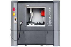
RX Solutions EasyTom 160 Multi-Purpose
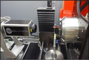
The tomographic analysis includes in most cases a global scan to locate the suspected components, followed by one or more local scans focused on these components at very high resolution.
The transition from the micro configuration, allowing to see the whole part, to the nano configuration, giving the image at a very high resolution of a particular component, is done in less than a minute. The targeted area can be defined on the global scan and then zoomed in for a very high-resolution scan. Centering is easy, even at very high resolution, thanks to a virtual rotation axis function centered on the area of interest.
Learn More?
Please click on ‘Request Application Note’ and we will send you the full application note ‘X-ray Computed Tomography for failure analysis in on-board electronics’.