
Smart nanostructured materials involve an extensive understanding of their morphology and chemical composition to develop novel designs. Optical and transport properties could be strongly dependent on the morphology of such nanomaterial. Additionally, one can broadly increase the capabilities of such nanostructure by mixing several chemical elements or compounds. Semiconducting oxides like nanowires, nanobelts or nanorods are part of the smart materials’ family which shows a wide range of applications, such as lasers, sensors, photocatalysts, solar cells, optical and mechanical resonators, biomedical and healthcare devices. In the past years, scientific studies were mainly published on synthesis, characterization, and applications of semiconducting oxide nanowires. A paper from Alonso- Ortis, M., et al., 2017, highlighted that the high aspect ratio and the surface of nanowires and nanoparticles influences both the physical- and chemical properties and their growth mechanism. Varley, J. B., et al., 2012, described that considering the physical properties of theses nanomaterials, it is a challenge to get efficient doping of oxide nanowires with controllable conductivity.
Spectroscopy techniques such as Raman, Photoluminescence and SEM-CL, play a key role for a comprehensive characterization of such complex and novel nanomaterial.
Thanks to the high specificity combined with a good spatial resolution, these techniques can bring crucial information for nanostructures’ investigations. The combination of these spectroscopic techniques can bring a lot of information about the studied sample. While Raman spectroscopy provides molecular composition and phase information, SEM-CL provides optical properties and doping, and SEM gives insights about the structure, elemental composition, and morphology of oxides. Further, Photoluminescence spectroscopy can be used to identify the band gap, homogeneity, impurity levels and defects.
However, a critical point on this type of study is the ability to measure a specific area or artefact at the same location through all the techniques available. Being colocalized, allows a comprehensive characterization of the sample and a precise superimposition of the images. HORIBA Scientific developed a new relocalization solution, called nanoGPS navYXTM. Based on the nanoGPS technology (Acher, O., et al., 2021). nanoGPS navYXTM can precisely relocalizes the specific areas in the sample from one instrument to the another with a high degree of accuracy, rapidly and easily.
In this application note, we present the key role of nanoGPS navYXTM as a relocalization tool for colocalized characterization of nanostructured materials and the advantages of Raman, Photoluminescence and SEM-CL correlated measurements.
Instrument and methods
Sample Preparation
In this work, a skewer-like heterostructure formed of a main longitudinal Ga2O3 nanowire decorated with SnO2 nanoparticles, was analyzed in depth. This architecture consists of a Ga-containing trunk with thicknesses between 50−150 nm for different skewers, surrounded by Sn containing rhombohedral-shaped particles. The source materials, pure Ga and tin oxide powders, were placed on the top of a gallium oxide pellet, which acted as the substrate, into an open tubular furnace. Skewer-like structures were extensively produced after 15 h of thermal treatment under an argon gas flux of 0.8 l/min. All samples were supplied for our experiments by Dr. Emilio Nogales Diaz from Universidad Complutense de Madrid.
nanoGPS navYXTM relocalization technology
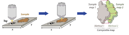
nanoGPS navYXTM is a relocalization method based on machine readable small-patterned tags fixed on the samples or their substrates. The patterns include an imaged-based position sensing technology, for which an image of a small part of the tag can automatically be interpreted into absolute coordinates and angular orientation. Taking a single snapshot on the tag with an imaging instrument provides the correspondence between sample and moving stage coordinates. This correspondence is a crucial information to guarantee the colocalization of the images by using different objectives or different instruments, bringing a huge benefit for the user, a full characterization of their sample at the same location (Figure 1).
Learn More?
Please click on ‘Request Application Note’ and download the full application note ‘Multimodal spectroscopy techniques for nanostructured materials characterization’.