
Introduction
A scanning electron microscope (SEM) is an instrument that detects the signal generated while scanning an electron beam across a specimen surface to image. The signals that can be obtained by electron beam irradiation include secondary electrons (SEs), backscattered electrons (BSEs), characteristic X-rays, and cathodoluminescence (CL), and since these make it possible to perform a detailed surface analysis of the sample, the SEM is used in a variety of fields from semiconductor device analysis to materials development.
However, when a nonconductive specimen is observed, the specimen surface becomes charged by the incident electrons, and imaging artifacts such as abnormal contrast and image drift occur. Low-vacuum SEM observation has been developed as a method to avoid or to mitigate these problems. In the low-vacuum SEM, positive charges generated by collisions between incident electrons and residual gas molecules inside the chamber act to neutralize the negative charge on the specimen surface, reducing the effect of charging.
Since it is difficult to detect low-energy SEs by observation in the low-vacuum range, Hitachi has developed an ultra variable-pressure detector (UVD) for the low-vacuum SEM, which can detect SEs under low-vacuum conditions1). In addition to the SE detector functionality, applications that utilize the features of this UVD were also developed. This paper describes examples of using the UVD for CL observations of materials and for scanning transmission electron microscope (STEM) observations of nanomaterials and liquid specimens.
Ultra Variable-pressure Detector (UVD)
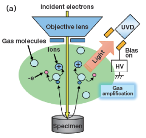
Figure 1(a) shows a schematic diagram of the UVD. In order to efficiently detect SEs generated from the specimen when it is irradiated by an electron beam under a low vacuum, a bias voltage is applied to the detector front edge.
This forms an electric field between the detector and the specimen, which accelerates the SEs generated at the specimen surface. The SEs then collide with the residual gas molecules in the low-vacuum environment, ionizing the molecules into positive ions and electrons while simultaneously generating light. By detecting this light using the UVD during the beam scanning, images that reflect topological information about the specimen surface can be captured.
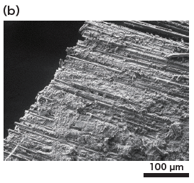
Figure 1(b) shows the results of observation of a fracture surface of carbon fiber reinforced plastic (CFRP) using a UVD mounted on a model SU3800 tungsten SEM (W-SEM) system.
The detailed surface roughness of the resin fracture surface and the state of the resin around the carbon fibers could be observed in the low-vacuum condition while suppressing charging. In order to respond to a wide range of needs, Hitachi have been able to provide the UVD in a range of microscopes from a W-SEM system equipped with a thermal electron gun to a field emission SEM (FE-SEM) system equipped with a Schottky electron gun.
CL Observation Examples Using the UVD
Since information such as the crystallinity and chemical properties of a specimen can be obtained by measuring CL, which is generated by irradiating the specimen with an electron beam, it is used for analysis of specimens such as semiconductors, ceramics, minerals, and fluorescent materials. The UVD is also capable of detecting CL information. CL images can be captured using the UVD by turning off the bias voltage applied to the detector front edge. As a result, the light that carries the secondary electron information as described in the previous section can no longer be detected, and only the CL signal generated from the specimen is detected. Figure 2 shows an example of observing crystal dislocations (defects) in gallium nitride (GaN) which is used in power semiconductors with a model SU5000 FE-SEM. When a GaN substrate is irradiated by an electron beam, areas of good crystallinity generate CL and appear bright, while areas containing threading dislocations do not emit light and appear dark. The black dots in Figure 2 correspond to areas where no light has been emitted due to the presence of dislocations, and this shows that dislocations in GaN can be clearly identified.
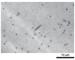
Fig. 2 CL observation results for gallium nitride substrate (accelerating voltage: 5 kV) (Specimen provided by courtesy of Associate Professor Yoshio Honda, Center for Integrated Research of Future Electronics, Institute of Materials and Systems for Sustainability, Nagoya University).
Learn More?
Please click on ‘Request Application Note’ and download the full application note ‘New Material Observation Method by SEM Using Ultra Variable-pressure Detector (UVD)’.