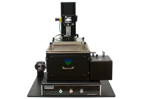
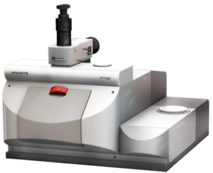
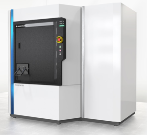
The LabRAM Odyssey Semiconductor microscope is the ideal tool for photoluminescence and Raman imaging on wafers up to 300 mm diameter. The HORIBA best-seller true confocal microscope is equipped with automated 300 mm sample stage and objective turret to fit both needs of wafer uniformity assessment and defects inspection.


 Key Features and Benefits
♦ Wafer mapping with automated turret and sample stage
♦ Uniformity measurement with wafer tilt correction
♦ From full wafer to high resolution defect mapping with DuoScan
Applications
♦ 2D Materials
♦ Group IV Semiconductors
♦ Compound Semiconductors
About HORIBA Scientific
HORIBA Scientific offers 200 years of experience in developing high-performance scientific instruments and analytical solutions. It’s a world-leading supplier providing researchers superior products and solutions, supported by a global network of service and application support.

Why HORIBA Scientific?
♦ Worldwide leader in analytical solutions
♦ 200 years of experience in R&D
♦ Research driven, leading-edge technology♦
♦ Complementary product range♦