Progress in end products such as smartphones, servers, automobiles and robots is driven by improvements in the performance of semiconductor devices. These improvements have been achieved not only through miniaturization but also by the introduction of three-dimensional structures and new types of memory.
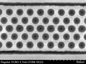
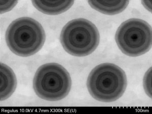
The figure below shows the SEM observation result of a plane surface of 3D NAND Flash Memory. The surface of memory area was flattened by mechanical polishing and Ar+ ion milling for FE-SEM (Regulus8200) observation. It shows distribution of memory cells arranged regularly at x100k magnification. The SiN, Poly-Si and SiO layers laminated concentrically in the memory cells were visible with high resolution and high contrast at x300k magnification.