
The Organic Photovoltaics group of the Karlsruhe Institute of Technology (KIT) studies the fabrication, optimization and simulation of organic solar cells and semiconductor devices. We focus on the evaluation of new materials, deposition techniques and device fabrication, including all steps from single layer deposition and structuring to device characterization. The task of this work was to build large-scale organic light emitting diodes (OLEDs) for luminaires. This required an invisible series connection of OLEDs to reduce the device current and hence to mitigate ohmic losses. A femtosecond laser was used to selectively structure the layers.
The high resistance of the semi-transparent electrodes in OLEDs lead to severe ohmic losses. The ohmic losses lead to inhomogeneous light emission from the device. The problem can be solved by connecting smaller OLEDs in series. The smaller area of the devices limits the current, hence decreasing the total power losses on the device while maintaining the same luminance. To monolithically connect the device in series three patterning steps are performed, henceforth referred to as P1, P2 and P3 (Figure 1). P1 electrically separates the bottom electrode. P2 allows the connection of the top and bottom electrodes and P3 separates the top electrodes. The area between this P1-P3 is does not emit light and should be minimized. Laser ablation is a proven method to structure P1, P2 and P3 and decrease the inactive area.
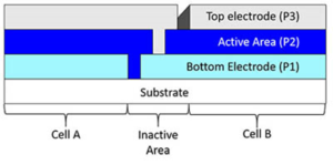
Figure 1. Subdivided devices using a monolithic connection. The three patterning steps P1, P2 and P3 are shown
Learn More?
Please click on ‘Request Application Note’ and we will send you the full application note ‘Laser structuring of organic optoelectric devices’.