
The CMP process
Chemical Mechanical Planarization (CMP) is one of the most critical processes in the semiconductor, hard disk and LED wafer manufacturing segments. The process is applied to assure the required planarity of the substrate wafer and for re-planarization at some intermediate points following deposition and lithographic processing for the structures built upon the wafer. In general, planarization is necessary to ensure functionality of the multi-level interconnects within the structures, but the technique is also commonly used to reduce wafer thickness whilst maintaining uniformity.
During the CMP process, the wafer is held on a rotating fixture and pressed against a rotating polishing pad while an abrasive chemical liquid (slurry) is distributed between the wafer and the pad. Pad rotation and concentric grooves engineered into the pad surface serve to transport the slurry across the interface between the pad and wafer. The chemical slurry weakens the surface of the wafer, thus enabling removal of material by asperities of the pad (figure 1) The quantity of material removed from the wafer and the quality of the overall process is highly influenced by the surface properties of the polishing pad. The surface of the pad degrades as a result of the polishing action, so it needs to be constantly reconditioned. Conditioning involves an abrasive process on the pad surface, where a rotating abrasive or conditioning disk recovers the pad surface. These disks are usually made of stainless steel or electroplated diamond.

Figure [1] CMP process schematic diagram

Figure [2] Wafer manufacturing without CMP (a) and with CMP (b)
Surface Metrology for CMP
The need for surface metrology for the CMP process is evident given that mechanical interaction between the surfaces is a critical variable for all stages of the process. The surfaces that need to be periodically characterized throughout the process include the conditioning disk surface, the wafer surface and the pad surface. In high volume production environments, however, non-destructive in-situ pad characterization at natural pauses in the polishing process (for example, when changing wafers) is desired. This would permit detection of drifts in key pad parameters and assist in validation of process changes. The goal in all cases is to extend the lifetime of consumables and to improve the yield of the whole process.

Figure [3] topography of conditioning disk surface
There are two main factors affecting pad surface degradation and lifecycle – pad groove occlusion and pad glazing.
Groove occlusion
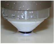
Figure [4] Immersion objective
Pad glazing
Glazing is a more complex phenomenon where the polishing ability of the pad is reduced due to surface degradation. This phenomenon enhances wear between wafer and pad, thus increasing process temperature and that may result in material selectivity during polishing. The phenomenon cannot be predicted as easily as groove occlusion and requires constant monitoring in order to guarantee ideal performance of the CMP process.
In order to enable in-situ pad surface monitoring, the metrology approach used must be able to work under wet conditions. Only immersion metrology can meet these requirements. The main benefit of this approach is that the pad does not need to be removed from the polisher in order to be characterized. This makes it possible to monitor pad glazing and groove occlusion in-situ at various points in the pad’s life-cycle. In-situ metrology has proven to extend pad lifetime, allowing operators to utilize the pads to the end of their useful life.
A new immersion metrology system
Working closely with experts in the field, Sensofar has developed the most suitable solution to solve this problem. The goal: change the polishing pads only when there is an absolute need, thus increasing yield per pad and minimizing downtime of the polishing systems.
The proposed solution is a non-destructive, in-situ metrology system, S mart CMP. Utilizing a portable stand, the sensor can be simply placed on the pad while the pad is still installed inside the polishing system and provides an immediate status on pad condition. S mart CMP is equipped with a laptop computer for enhanced portability and has been designed to work both as a stand-alone sensor and alternatively as a system that can be integrated into the production line as an automatic metrology solution. In both cases, S mart CMP is capable of rapidly acquiring and analyzing data in order to effectively monitor key pad characteristics.
This solution has already been proven to successfully monitor pad glazing and groove occlusion. Thanks to S mart CMP it has been clearly demonstrated that CMP pads are largely under-utilized and are often discarded with more than half of the useful lifetime still remaining.

Figure [5] S mart CMP, 3D optical sensor
Go to ‘request application note’ and download the full application note.