Table Of Contents
How does AFM-IR/PiFM work?
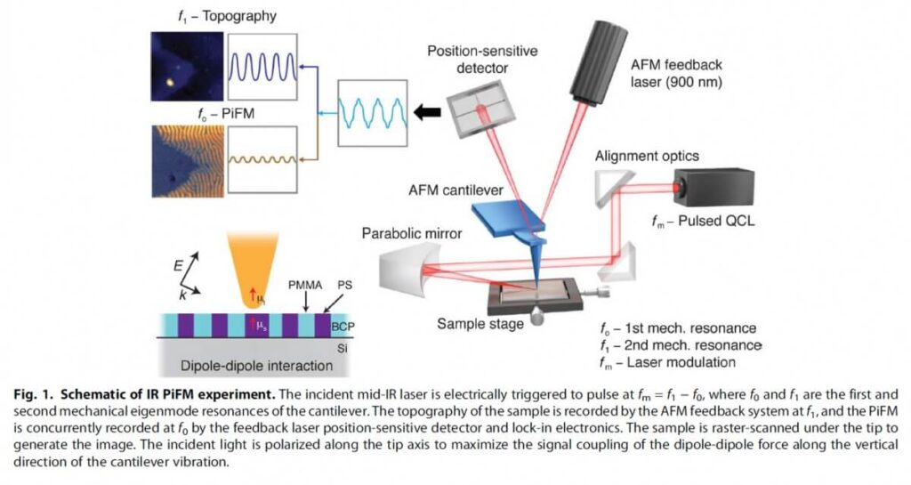
In AFM-IR or nanoIR, the atomic force tip scans the sample while an infrared laser excites the sample to facilitate IR spectroscopy. Thus, both the topography and the chemical spectra are recorded with high resolution. There are several ways to measure the IR absorption spectra through the AFM tip. In PiFM, the photoinduced force is the result of a dipole-dipole force attraction between the imaging tip and the sample when illuminated with a monochromatic, coherent light source.
Through imaging at multiple IR wavelengths, corresponding to absorption peaks of different chemical species, PiFM has the ability to spatially map nanometre-scale patterns of the individual chemical components. A schematic diagram of PiFM is shown below:
Why use AFM-IR/PiFM?
Compared to competing AFM-IR techniques, photo-induced force microscopy has several advantages. For example, in photo-thermal AFM-based techniques, the thermal expansion in the sample can reduce the spatial resolution and surface sensitivity. For scattering SNOM type AFM-IR techniques the spatial resolution and surface sensitivity are good but important challenges remain in the interpretation of the images, the extraction of useful information from the background and the presence of artefacts in the optical image.
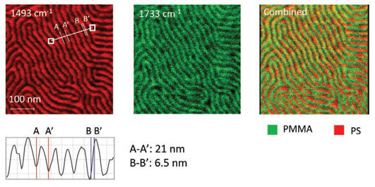
PiFM has an excellent signal to noise ratio and a small interaction volume, leading to increased spatial resolution. It is for example possible to resolve the different chemical blocks of a PS-b-PMMA block copolymer sample with a pitch of about 22 nm (the rise of the signal / resolution measures less than 7 nm).
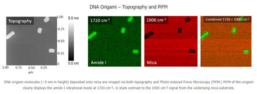
Excellent surface sensitivity is demonstrated in the DNA origami measurement below. Especially the image at 1000 cm-1 which highlights Mica shows that the technique does not measure the Mica under the 3nm DNA patch.
Finally, PiFM does not suffer from background interference and shows a good correlation with conventional IR-spectra from bulk materials without sample thickness effects.

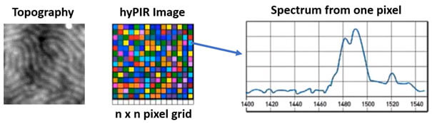
A powerful way to analyse unknown samples is hyperspectral AFM-IR imaging (hyPIR), providing images of all the resonant modes in a structure with a single scan. A 128 by 128 pixel grid can be produced in about one hour.
PiFM examples
Using Infrared photo-induced force microscopy you will be able to acquire IR spectra while simultaneously mapping topography. Infrared wavelengths specific to different chemical entities resolve the nanometre-scale distribution of each chemical species in diverse multi-phase and multi-component systems.
For example, hyperspectral infrared PiFM will give you a quick idea about the chemical makeup of perovskite photovoltaic films, which have a complicated domain structure. The scan shows different chemical phases and chemical transitions across phase boundaries.
DNA origami molecules (~3 nanometre in height) deposited onto mica are readily imaged via both topography and PiFM. The signal of the DNA molecules clearly shows the amide I vibrational mode.
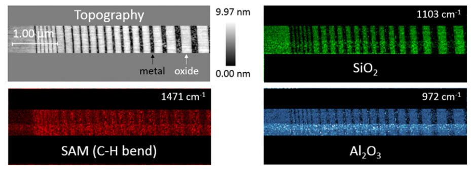
For many semiconductor applications, PiFM is a viable tool for, amongst others, the visualization and analysis of area selective deposition (ASD / Image below), local strain, the cross-section of a trench, the cross-section of a multilayer stack, chemical mechanical polishing (CMP), buried conductive layers and defect analysis.
As the future of materials science is nano, photo-induced force microscopy (AFM-IR) is an indispensable tool to analyse the topology and chemical makeup of new materials in exquisite detail.