Introduction
Scratch Testing is a widely used method to evaluate the adhesion and scratch resistance of coated surfaces. The procedures to quantify the adhesive and cohesive strength of hard coatings, requires the definition of “critical load” values. These values are associated to the characteristic failure events at where a coating will start to show delamination or cohesion failure. A stylus is drawn across the coating or thin film surface, while a gradually increasing load is being applied. In traditional scratch testing, cohesive and/or adhesive failure is detected by measuring friction force, scratch depth, acoustic emission or electrical contact resistance in combination by observation under a 2D optical microscope. In the event of thick and multi-layered coatings, this 2D observation works well when adhesion properties are not close to each other. However, with the next generation coatings and thin films, the traditional method doesn’t always provide differential results to distinguish the cohesion and adhesive properties.
3D Scratch Testing
In order to obtain high resolution images of the scratch test which is generated, the Rtec Instruments UST-2 system combines a dedicated scratch tester with a high resolution 3D Profilometer. A typical 3D Scratch Test involves the automated acquisition of surface roughness, thickness and topography before and after a scratch is generated.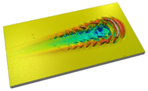
After the sample is mounted in the sample holder on the scratch tester, it moves with the XY stages under the 3D Profilometer (Confocal & Interferometer) to evaluate surface topography. After acquiring the topography image of the sample surface, it moves back to the scratch module to conduct the scratch at the pre-defined test conditions. Again, the sample moves back to the 3D Profilometer module and takes a 2nd image of the surface (which now contains the scratches).
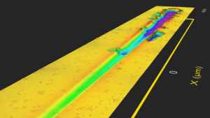
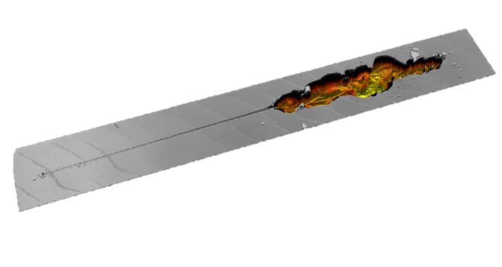
The analysis software synchronizes the data of friction force, normal load, displacement, acoustic emission and electrical contact resistance with the high resolution 3D image. This full-automated test sequence provides the user correlation of adhesion and hardness with surface roughness and topography. The images which are generated provide valuable details of the scratch / wear track with complete information of cracks propagation, scratch width, volume, pile-up and self-healing behaviour.
In comparison to the traditional scratch tester with light microscope, the 3D Scratch Tester has major advantages for higher accuracy and user-independent scratch analysis:
- Scratch testing with high accuracy with 3D Optical Profilometer
- Comprehensive analysis of deformation and failures during the scratch test
- Non-contact imaging of scratch track and visualization of self-healing behaviour
- More details of surface and fracture by using Confocal Microscopy
- Synchronized data with full 3D panorama profile of the scratch
Applications
Interchangeable scratch modules allow a wide range of applications: from thin layers with a thickness of a few nanometers to hard and thick coatings with thicknesses of several mm. The required load range is mainly depending on the coating thickness and hardness of the coating. 4 modules are available which can be interchanged by the user in less than 2 minutes: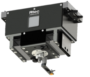
- Nano Scratch Testing for coatings and thin films <1000 nm
- Micro Scratch Testing, normal load range up to 50N
- Macro Scratch Testing up to 200N for hard coatings
- Heavy Duty Scratch Testing for scratch resistance of hard materials and thick coatings >200µm
Coatings and thin films can be seen everywhere for protection, decoration, lubrication, optical and many more functional properties. From industrial thin films in plasma processed layers in semiconductor and optical lenses, to decorative and protective coatings in consumer goods and automotive parts. In machining, cutting, forming, punching, stamping and several other industries, hard coatings are applied to improve lifetime and precision for energy savings and longer service intervals.
Examples of application:
- Automotive: Paint, varnishes, pistons, engines, brake pads, windows, …
- Hard Coatings: TiN, WC, DLC, cutting tools, PVD, CVD, thermal spray,..
- Bio Materials: Implants, stents, bone, tissue, tablets, artificial joints,…
- Materials: Ceramics, polymers, metals, rubber, composites
- Semiconductor: thin films, Low-K, passivation layers, MEMS, NEMS, hard disks
- Optical: Eye glass, lenses, AR Coatings, mirror, touch screen, display panels,…
- Decorative: Jewellery, watches, cases, anti-corrosion coatings


Micro Scratch Tester: Progressive scratch on automotive paint with damage to clear coat simulating common scratches on cars.
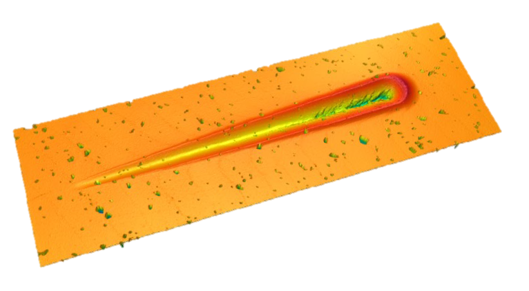
Nano Scratch Tester: Progressive scratch test on a smartphone screen exhibiting good scratch resistance prior to catastrophic failure.