
In this case study, Linkam and Sensofar Metrology demonstrate their collaboration in producing and experimental setup for temperature-controlled optical profilometry experiments. This had historically been a difficult procedure due to imaging issues caused by spherical aberrations. Using Linkam’s precision temperature control chamber with Sensofar’s Linnik objective lens eliminates these problems and allows accurate measurement of 3D topographic profiles of nanoscale materials. Here, we observe the changes in topography of silicon wafers as they evolve with temperature from 20°C up to 380°C.
Rapid Thermal Processing (RTP) is an important step in the the manufacturing process of silicon wafers, in which the wafer is rapidly heated to high temperatures for a short period of time, then slowly cooled in a controlled manner, in order to impart the desired semiconducting properties to the wafer. However, RTP, causes thermal stress which leads to other problems in photolithography that may affect the performance of the device, such as breakage due to thermal shock or dislocation of the molecular lattice. Understanding the behavior of a wafer under these conditions can help optimize the process, improving semiconductor properties and wafer durability.
Experimental details
In this work, we study the effect of the RTP process on the silicon wafers while accounting for optical aberrations brought about by temperature changes. Two different samples were used, corresponding to different chip designs from silicon wafers. Sample A was 2.8 mm x 1 mm in size, whereas Sample B was 3.0mm by 2.35 mm. Silicon wafers have typical surface roughness values on the sub-micron scale, so the ideal optical technology for this application is Coherence Scanning Interferometry (CSI, ISO 25178, part 604). CSI offers only 1 nm of system noise, regardless of the magnification of the lens being used.
For the design and construction of the Linnik objective, two Nikon 10x EPI objectives (Nikon, MUE12100) with 17.5 mm working distance were used. The same configuration is available with 10xSLWD objectives (Nikon, MUE31100), providing a 37 mm working distance. This makes the thermal emissions from the camera almost imperceptible to the lens and will not affect or damage the measurement quality. The Linnik objective was mounted on the 3D optical profilometer (Sensofar, S neox) , which combines 4 optical technologies in the same sensor head: Confocal, CSI, PSI and focus variation. These techniques are covered in ISO25178.
The temperature is controlled using a Linkam LTS420 chamber and the T96 temperature controller, which allows the temperature to be ramped and controlled between -195° and 420 °C to a precision of 0.01°C, while the sample roughness is observed through the chamber window. The chamber also allows control of the pressure and humidity, but this has not been investigated in this study.
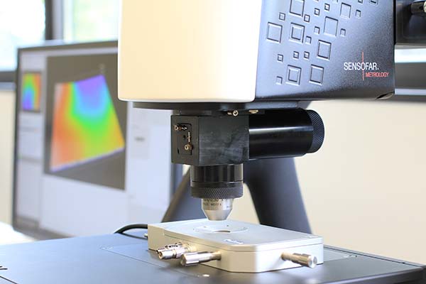
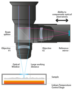
Figure [2] Experimental setup of Linkam LTS420 and Sensofar Linnik configuration. Schematic of the Linnik Optical Configuration
Learn More?
Please click on ‘Request Application Note’ and download the full application note ‘Characterizing the temperature-induced evolution of the shape and texture of a silicon wafer’.