
How does ion milling work?
Ion milling is a precision material removal technique used in microscopy and materials science. In ion milling, a high-energy ion beam, typically composed of argon ions, bombards a sample’s surface at a controlled angle. These ions sputter away surface atoms, gradually etching a thin layer of material. By adjusting parameters like ion energy and angle of incidence, researchers can precisely control the milling rate and depth. This process creates a flat, polished cross-section of the sample for microscopic analysis, revealing its internal microstructure and features. Ion milling is invaluable for preparing samples, especially those with delicate or heat-sensitive materials, for electron microscopy and other analytical techniques.
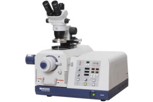
The ion milling systems manufactured by Hitachi High-Tech apply a broad low-energy Ar+ ion beam to sputter sample material. Cryogenic ion milling is even possible for heat sensitive samples to reduce damage by beam irradiation. Both systems, the IM4000II and the ArBlade5000 are hybrid models suitable for two different milling configurations: cross section milling and flat milling.
Cross section milling:
A mask is placed directly on top of the sample. This protects the top surface and provides a sharp edge to create a polished cross section by sputtering material away that is exposed beyond the edge of the mask.
Flat milling:
The argon ion beam has a Gaussian-shaped current profile and material removal rate is therefore higher at the center of the beam than at the surrounding area. For this reason, the ion beam center is eccentric from the sample rotation center. As the sample rotation and swing center are varied with respect to the ion beam center, a wide area can be sputtered uniformly.


Why use ion milling?
Ion milling, also called broad ion beam (BIB) ion milling is a widely used physical preparation technique for producing high-quality surfaces for scanning electron microscopy (SEM). The method employs a broad, low-energy beam of inert gas ions—typically argon—to gently sputter material from the specimen surface under vacuum.
The primary reason to use ion milling is to obtain a damage-free, deformation-free surface. Conventional mechanical polishing can introduce scratches, smearing, and subsurface strain, especially in hard, brittle, or heterogeneous materials such as ceramics, composites, and metals with multiple phases. Ion milling removes these mechanically induced artifacts by sputtering atoms directly from the surface, resulting in a flat, smooth area suitable for high-resolution imaging and microstructural analysis.
Another important advantage is the ability to prepare cross sections of multilayered or composite samples without causing distortion at material interfaces. By tilting and rotating the specimen during milling, uniform material removal can be achieved even across regions with different hardness or composition. This makes the ion milling method particularly valuable for analyzing coatings, thin films, and interfaces where conventional polishing might cause delamination or rounding of edges.
Ion milling is also used for final surface finishing after mechanical polishing. A short ion polishing step can effectively remove residual contamination, oxide layers, and polishing debris, improving contrast and analytical accuracy in SEM, EDX and EBSD.
Furthermore, because the technique operates without mechanical contact, it is suitable for fragile or irregularly shaped specimens that might otherwise be damaged by physical preparation.
Even though Hitachi’s ArBlade5000 is the fastest ion miller on the market, the process is relatively slow and limited to small surface areas, so it is typically employed as a final preparation step rather than a bulk material removal method. Despite this limitation, broad ion beam milling remains a critical technique wherever high surface integrity and microstructural fidelity are required.
Advantages and limitations of ion milling
There are several advantages and limitations to using ion milling. The most prominent are listed below.
Advantages
- Damage-free surface preparation
Unlike mechanical polishing, ion milling removes material through sputtering rather than abrasion. This minimizes mechanical stress, strain, and deformation in delicate materials such as ceramics, composites, and multilayer thin films. - High surface quality and planarity
Ion milling can produce extremely smooth, scratch-free surfaces, making it ideal for high-resolution imaging and microstructural analysis in SEM or TEM. - Controlled material removal
The process allows precise control over milling rate and area, enabling selective thinning or cross-sectioning of specific regions of interest. - Suitable for hard or brittle materials
Materials that are difficult to polish mechanically—such as hard metals, semiconductors, or brittle ceramics—can be effectively prepared using ion milling. - Cleaning and contamination removal
Gentle ion polishing can remove surface oxides, residues, or contaminants introduced during cutting or polishing steps, improving imaging and analytical accuracy.
Limitations
- Slow material removal rate
Ion milling is generally a time-consuming process, particularly when large areas or thick layers need to be removed. - Surface artifacts due to redeposition or ion damage
Prolonged milling or high ion energies can cause surface amorphization, ion implantation, or redeposition of sputtered material, leading to artifacts that may interfere with surface-sensitive analyses. - Thermal and charging effects
Non-conductive samples can accumulate charge under ion bombardment, and localized heating may alter sensitive materials or cause diffusion of elements. - Limited area coverage
The effective milling area is typically small, making the technique less suitable for preparing large or bulk samples. - Cost and equipment complexity
Ion millers are relatively expensive and require vacuum systems, precise alignment, and maintenance, which may limit accessibility.
Types of ion milling
Several ion milling techniques are available, each offering distinct advantages depending on the material type, area size, and level of precision required.
Broad Ion Beam (BIB) ion milling
Broad Ion Beam (BIB) ion milling uses a wide, low-energy beam of inert gas ions—most commonly argon—to gently sputter material from the surface. Because the beam covers a relatively large area and the sample can be tilted or rotated, it produces highly uniform, deformation-free surfaces. This makes BIB milling ideal for final surface polishing and cross-section preparation for SEM or EBSD, particularly when mechanical polishing introduces scratches or strain.
Focused Ion Beam (FIB) ion milling
Focused Ion Beam (FIB) ion milling employs a finely focused, high-energy ion beam—typically gallium or xenon—that can be scanned across the surface with nanometer precision. FIB systems allow site-specific material removal, imaging, and patterning, making them indispensable for preparing TEM lamellae, micro- and nanostructures, and precise cross-sections of small features. Dual-beam FIB-SEM instruments combine ion milling with SEM imaging for in situ monitoring and control.
Cryo-Ion milling
Cryo-Ion milling is performed at cryogenic temperatures to minimize heating and beam-induced damage. This approach is especially valuable for polymers, biological specimens, and other beam-sensitive or volatile materials, where conventional ion milling could cause structural changes, melting, or evaporation. Cooling the specimen preserves its native microstructure and prevents unwanted modifications during sputtering.
Plasma FIB ion milling
Plasma FIB ion milling represents a more recent development that replaces the traditional gallium ion source with a plasma-based source, such as xenon or argon. Plasma FIB systems can deliver much higher ion currents, allowing for faster removal of large volumes of material while maintaining good surface quality. This makes them well-suited for large-area cross-sections, 3D tomography, and the preparation of bulk samples that would be impractical to process with standard FIB systems.
Together, these methods provide a flexible toolkit for preparing a wide range of materials for electron microscopy, from delicate thin films to bulk, hard, or composite samples, each technique balancing precision, speed, and surface integrity in different ways.
Applications of ion milling
Relief ion milling vs flat ion milling
Because of the Gaussian-shaped argon beam, it is possible to emphasize topographical information of composite materials (relief ion milling) or to reduce surface topography for enhanced crystal orientation visualization (flat ion milling) by adjusting the beam irradiation angle.
Flat ion milling at an oblique angle minimizes the dependence betweensputtering rate and crystal orientation, yielding reduced surface topography and a flat sample surface. If the topography of composite materials is of interest, relief ion milling is applied. By sputtering perpendicular to the sample surface, convex and concave surfaces appear caused by compositional differences or grain orientations.
Electron backscatter diffraction (EBSD)
EBSD is a characterization technique used to study the crystal orientation and material phases within the sample. Within a SEM, the primary electron beam interacts with a tilted crystalline sample. Electron diffraction occurs and these electrons interact with a phosphor screen to become fluorescent. These signals are detected and a characteristic diffraction pattern is obtained. Slight variations in surface height change the angle of incidence of the electrons, thereby effecting diffraction patterns. For that reason, flat ion milling is typically utilized as sample preparation technique to obtain flat surfaces for EBSD measurements.
Powders
Cross-section polishing of powdered materials is a vital technique with diverse applications. It involves preparing polished surfaces within powders for microscopic analysis. In materials science and metallurgy, it aids in characterizing materials, detecting defects, and improving product quality. In pharmaceuticals, it ensures medication uniformity and safety. Industries rely on it for quality control, while it’s essential in failure analysis for structural assessment. Geological and environmental researchers use it to study samples, and it supports R&D efforts. In forensics, it helps identify trace evidence. This versatile technique plays a pivotal role in enhancing quality, safety, innovation, and knowledge across various fields.
Even the inside from individual powder particles are revealed with cross section polishing. If a sufficient amount of powder is mixed with epoxy and cured, the new block can be cut and processed with the ion miller. In battery research, powder analysis is common practice. Catalysts and cathodes are analyzed to improve their performance. The following image shows hollow zirconium shells containing one active nanoparticle.


