Dynamic random-access memory (DRAM) cells consist of a capacitor and transistor. Electrical charge is either stored or released from circular capacitors, controlled by the transistor. For economical motivations, the capacitors are packed in dense arrays to reduce DRAM surface area. High resolution SEM images are essential for plan view observations of DRAM capacitors. In order to obtain such high resolution SEM observations, sample preparation is necessary. In this application note, samples are prepared by relief and flat milling with an ArBlade5000 ion milling system before SEM imaging to get clean and flat surfaces. Subsequently, high resolution SEM images are acquired by Hitachi’s SU9000 Cold Field Emission (CFE) SEM to gain information about this capacitor packing. More detailed structures of each layer are visible after lamella preparation with the NX2000 FIB SEM.
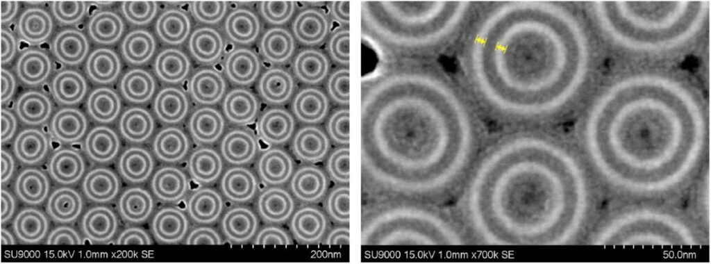
Figure 1. High resolution SEM observation of DRAM capacitors
Figure 1 shows plan view SE-images of densely packed DRAM capacitors with x200K and x700K magnifications after 100 minutes of relief milling and 8 minutes of flat milling. On the left image, circular capacitors were confirmed in regular arrangement. The inside of each capacitor consists of several concentric multi-layered rings of about 6 nm thick, as indicated with yellow arrows in the right image. To observe these rings in more detail, a lamella sample was prepared with FIB SEM for high resolution STEM imaging. The SU9000 is also a powerful low-kV STEM and allows for simultaneous brightfield and darkfield imaging. Figure 2 shows BF-STEM (a, c) and DF-STEM (b, d) images of the DRAM capacitors. The multilayered structure of approximately one to several nm (Fig. 2d, yellow arrow) thickness is clearly identified in this high resolution observation.
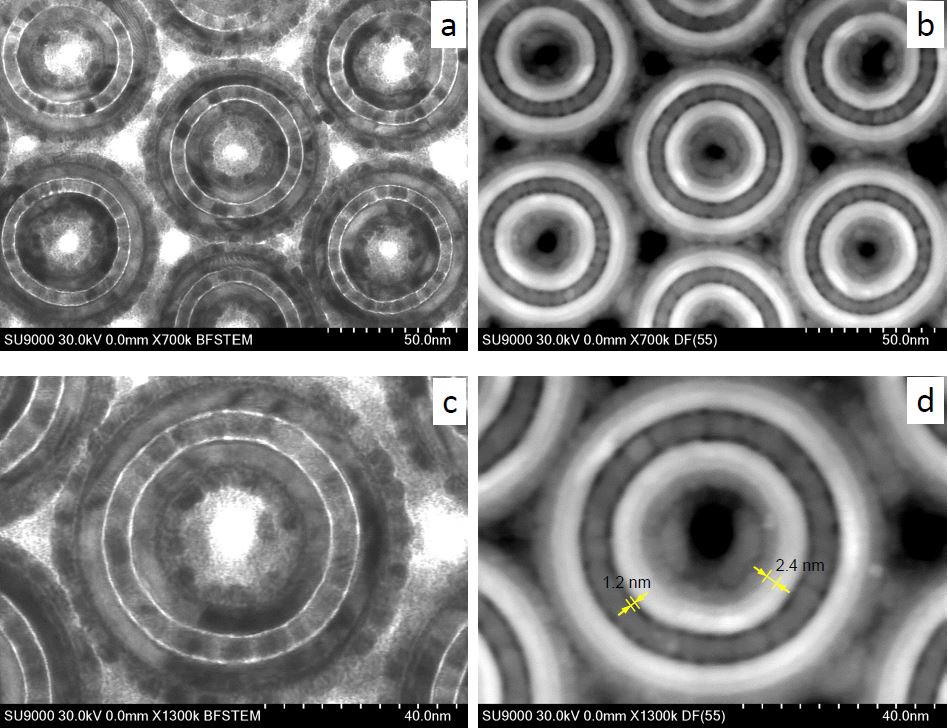
Figure 2. STEM observation of DRAM capacitors after lamella preparation
Additionaly, high resolution EDX mapping results are obtained with a windowless 100mm² EDX detector after 7 minutes of acquisition (Figure 3). Approximately 1 to 6 nm width element distributions are identified and concentric multi-layered structures consisting of SiGe, TiN and ZrO2 could be confirmed.
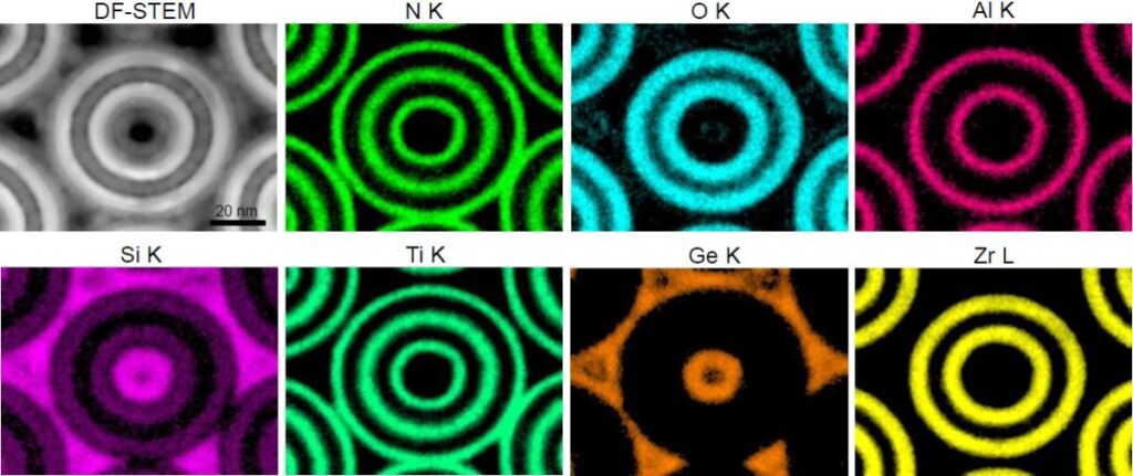
Figure 3. The SU9000 CFE SEM allows users to do EDX analyses with a high spatial resolution of several nm
Hitachi’s SU9000: Ultra high resolution SEM based on cold field emission technology
The new CFE gun technology featured in the SU9000 is the solution for high resolution SEM imaging: thanks to a high source brightness and low energy spread this system has the highest possible system (SE) resolution of 0.4 nm at 30kV. For more beam sensitive materials, this system offers an in-lens objective lens to improve low voltage imaging and to achieve high resolution SEM images without deceleration technology.