Physical Vapor Deposition


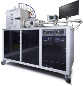
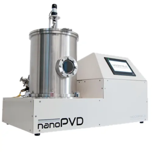
Physical Vapor Deposition (PVD) is a prominent thin-film coating technique used across industries like electronics, optics, and aerospace. In PVD, a solid material is vaporized within a vacuum environment. The vaporized atoms or molecules then travel and deposit onto a substrate, forming a thin film. PVD encompasses methods like sputtering and evaporation. Sputtering involves ion bombardment of a target material, releasing particles that coat the substrate. Evaporation relies on thermal energy to vaporize the source material for condensation onto the substrate. PVD offers benefits including precise thickness control, coating adherence to complex shapes, and material property enhancement. It’s pivotal for functional coatings, hardness improvement, optical enhancements, and conductivity modifications. PVD coatings are vital in semiconductors, solar cells, medical devices, and more, enabling tailored material characteristics.

MiniLab

Flexible, modular PVD systems for high quality R&D and pilot-scale production.

♦   MiniLab 026 | Compact, floor standing system

♦   MiniLab 060 | Moorfield’s most popular system

♦   MiniLab 080 | Tall chamber, ideally suited for thermal, LTE & E-beam

♦   MiniLab 090 | Glovebox Compatible

♦   MiniLab 125 | Pilot-scale, modular system

nanoPVD

nanoPVD

High-performance, high-vacuum benchtop PVD systems


♦   nanoPVD-T15A | R&D Scale Object Coating

♦  nanoPVD-ST15A | Compact benchtop high-performance, for thermal evaporation and magnetron sputtering

♦   nanoPVD-S10A-WA | Wide area configuration

♦   nanoPVD-S10A | Benchtop RF and DC magnetron sputtering

♦   nanoEM | Coating tool with a full research-grade feature set

How does Physical Vapor Deposition work?

Physical Vapor Deposition (PVD) is a sophisticated thin-film coating process used across industries for enhancing material properties and creating functional surfaces. PVD involves several fundamental steps:


  • Evaporation or Sputtering: PVD starts with the transformation of a solid material, known as the target or source material, into a vaporized state. This can be achieved through two primary methods: evaporation and sputtering.
    • Evaporation: The source material is heated to a high temperature within a vacuum chamber. The heat causes the material to vaporize and form a cloud of atoms or molecules.
    • Sputtering: In this technique, a high-energy ion beam is directed at the target material. The impact of ions on the target dislodges atoms from its surface, which then vaporize and form a cloud of particles.


  • Vapor Transport: The vaporized atoms or molecules generated through evaporation or sputtering travel freely within the vacuum environment. This vapor cloud contains the material that will form the coating.


  • Deposition onto Substrate: The vapor cloud is directed toward a substrate where the coating is to be deposited. The substrate is typically placed in close proximity to the vapor source.


  • Coating Formation: Upon reaching the substrate, the vaporized atoms or molecules lose their energy and condense onto the substrate’s surface. As they condense, they form a thin film that adheres to the substrate. This thin film is composed of the same material as the source/target material.


  • Film Growth and Control: The deposition process continues until the desired thickness of the thin film is achieved. Precise control mechanisms, such as monitoring the deposition rate and adjusting the process parameters, ensure that the coating reaches the intended thickness and uniformity.


  • Coating Properties: The characteristics of the deposited coating, including its thickness, composition, and microstructure, are influenced by factors such as the vaporization method, vacuum conditions, substrate temperature, and more.


PVD offers several advantages, including the ability to control coating thickness, even on complex shapes, and to enhance material properties like hardness, corrosion resistance, and optical properties. It is used in a wide range of applications, from creating protective layers on cutting tools to producing decorative finishes on various items. PVD’s versatility makes it a key technology in tailoring material surfaces to meet specific functional and aesthetic requirements.

Why use Physical Vapor Deposition?

Physical Vapor Deposition (PVD) is a favored coating technique due to its numerous advantages and versatile applications. Here’s why one would choose to use PVD:


  • Tailored Surface Properties: PVD allows precise control over coating thickness and composition, enabling customization of material properties to meet specific requirements. This is crucial for enhancing properties like hardness, wear resistance, and corrosion resistance.


  • Complex Geometries: PVD coatings adhere uniformly even on intricate shapes and complex geometries, which is challenging for many other coating methods. This makes PVD suitable for coating components with varying shapes and sizes.


  • Improved Material Performance: PVD coatings can significantly improve the performance of materials. For instance, tools with PVD coatings exhibit enhanced cutting efficiency and longer lifespan due to increased hardness and wear resistance.


  • Aesthetic Enhancement: PVD offers decorative finishes with unique colors and reflective properties, making it popular for jewelry, watches, and architectural elements. The process provides both durability and visual appeal.


  • Consistency and Uniformity: PVD ensures uniform coating distribution, resulting in consistent material properties across the entire coated surface. This is crucial for applications where evenness is essential.


  • Environmental Friendliness: PVD is a relatively environmentally friendly process compared to some other coating methods. It doesn’t require the use of harsh chemicals and produces minimal waste.


  • Compatibility: PVD coatings are compatible with a wide range of materials, including metals, ceramics, and polymers. This versatility allows PVD to be used in various industries and applications.


  • Microelectronics and Semiconductors: PVD plays a critical role in producing microelectronic devices and semiconductors, where precise, uniform, and controlled coatings are essential for device performance.


  • Optics and Optoelectronics: PVD is used to create optical coatings for lenses, mirrors, and other optical components. These coatings enhance light transmission, reflection, and absorption properties.


  • Medical Devices: PVD coatings provide biocompatibility and wear resistance to medical implants, improving their performance and longevity within the body.


  • Energy Efficiency: PVD coatings can be used in solar cells and energy-efficient windows to enhance their light-absorption and heat-reflective properties.


In summary, PVD is chosen for its ability to tailor material properties, coat complex shapes, improve performance, and achieve aesthetic finishes. Its versatility makes it applicable to various industries, contributing to enhanced product functionality and quality.

Applications for Physical Vapor Deposition

  • Cutting Tools and Tool Coatings: PVD-coated cutting tools play a crucial role in machining processes. These coatings, such as titanium nitride (TiN) or titanium carbonitride (TiCN), enhance tool hardness and wear resistance. By reducing friction and preventing tool wear, PVD-coated tools maintain sharpness and extend tool life. This application is vital for industries like aerospace, automotive, and manufacturing, where efficient and precise machining is essential.


  • Decorative and Architectural Finishes: PVD is widely utilized for creating durable and aesthetically appealing decorative finishes. Watches, jewelry, and fashion accessories benefit from PVD coatings that offer unique colors and high scratch resistance. In architecture, PVD-coated metal surfaces are used for building facades, interior design elements, and fixtures. The coatings provide both visual appeal and long-lasting protection against environmental factors.


  • Microelectronics and Semiconductors: PVD is indispensable in microelectronics for depositing thin films critical to device functionality. Metalization layers like aluminum and copper are deposited using PVD to form electrical connections between components. PVD is also used to produce diffusion barrier layers that prevent unwanted interactions between metals and silicon. These precise and conformal coatings are essential for ensuring the reliability and performance of microelectronic devices.


  • Optical Coatings: PVD coatings are integral in optics and optoelectronics. Anti-reflective coatings deposited on eyeglasses, camera lenses, and optical components reduce glare and enhance light transmission. Reflective coatings, such as aluminum or silver, create mirrors with controlled reflectivity. PVD coatings are also used in lasers, optical filters, and photovoltaic cells, influencing light propagation and absorption properties.


  • Advanced Materials Synthesis: Researchers use PVD to synthesize advanced materials with tailored properties. Diamond-like carbon (DLC) coatings, composed of amorphous carbon with properties resembling diamond, offer exceptional hardness, wear resistance, and low friction. These coatings find applications in biomedical devices, industrial equipment, and more. PVD-grown nanomaterials, such as nanowires and quantum dots, are investigated for their unique electronic and optical properties, contributing to advancements in nanotechnology and material science.